- 您现在的位置:买卖IC网 > PDF目录65534 > ICS9112YF-17-T (INTEGRATED DEVICE TECHNOLOGY INC) PLL BASED CLOCK DRIVER, 8 TRUE OUTPUT(S), 0 INVERTED OUTPUT(S), PDSO16 PDF资料下载
参数资料
| 型号: | ICS9112YF-17-T |
| 厂商: | INTEGRATED DEVICE TECHNOLOGY INC |
| 元件分类: | 时钟及定时 |
| 英文描述: | PLL BASED CLOCK DRIVER, 8 TRUE OUTPUT(S), 0 INVERTED OUTPUT(S), PDSO16 |
| 封装: | 0.150 INCH, MO-137, SSOP-16 |
| 文件页数: | 4/8页 |
| 文件大小: | 108K |
| 代理商: | ICS9112YF-17-T |
4
ICS9112-17
0051J—02/05/04
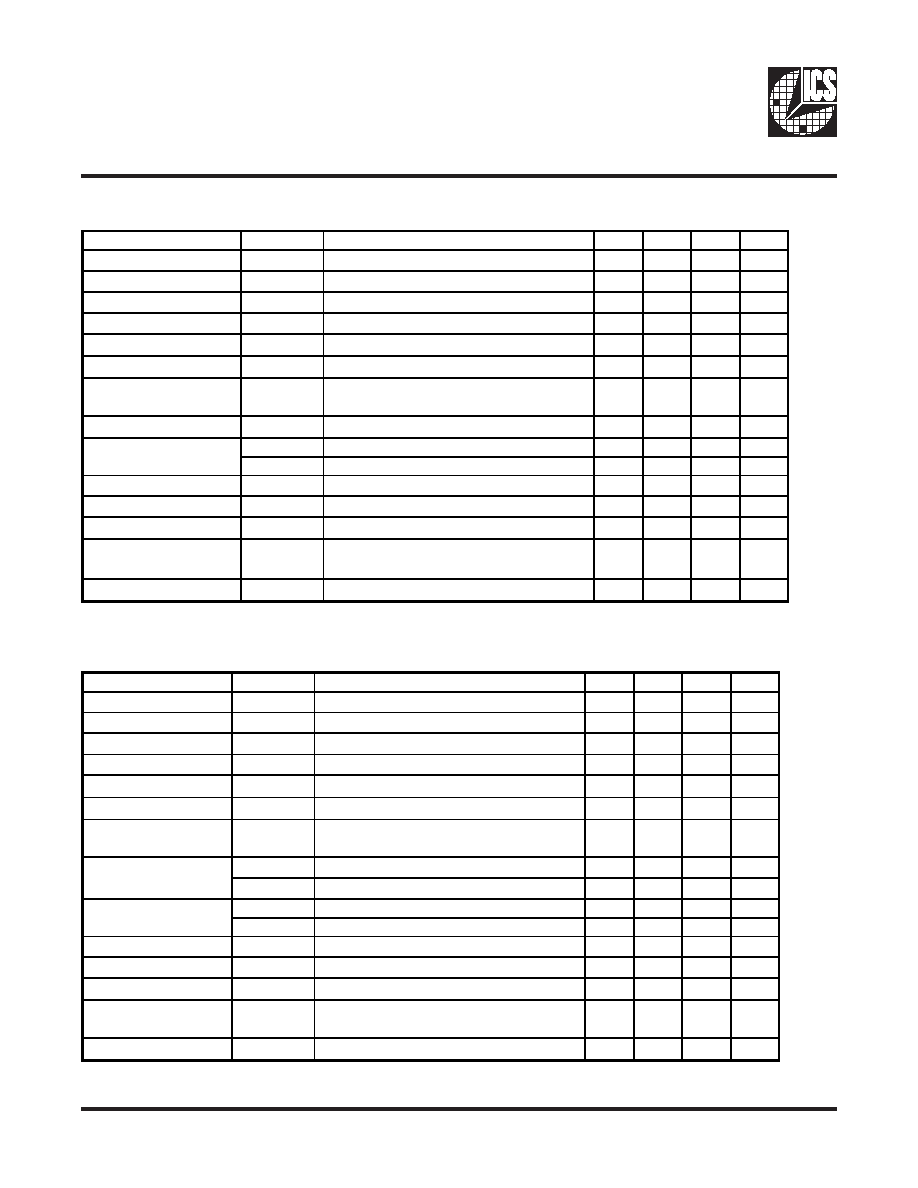
Electrical Characteristics - OUTPUT
TA = 0 - 70°C; VDD = VDDL = 3.3 V +/-10%; CL = 20 - 30 pF (unless otherwise stated)
PARAMETER
SYMBOL
CONDITIONS
MIN
TYP
MAX UNITS
Output Impedance
RDSP
VO = VDD*(0.5)
10
24
Output Impedance
RDSN
VO = VDD*(0.5)
10
24
Output High Voltage
VOH
IOH = -8 mA
2.4
2.9
3.3
V
Output Low Voltage
VOL
IOL = 8 mA
0.25
0.4
V
Rise Time
1
Tr
VOL = 0.8 V, VOH = 2.0 V
1.2
2.0
ns
Fall Time
1
Tf
VOH = 2.0 V, VOL = 0.8 V
1.2
2.0
ns
PLL Lock Time1
tLOCK
Stable power supply, valid clock
presented on REF pin
1.0
ms
Dt
VT = 1.4V;Cl=30pF
40
50
60
%
Dt
VT = Vdd/2; Fout <66.6MHz
45
50
55
%
Tcyc-cyc
at 66MHz , Loaded Outputs
250
ps
Tcyc-cyc
>66MHz , Loaded Outputs
200
ps
Absolute Jitter
1
Tjabs
10000 cycles; Cl=30pF
-100
70
100
ps
Jitter; 1-Sigma
1
Tj1s
10000 cycles; Cl=30pF
14
30
ps
Skew
1
Tsk
VT = 1.4 V (Window) Output to Output
250
ps
Device to Device Skew
1 Tdsk-Tdsk
Measured at VDD/2 on the CLKOUT
pins of devices
0700
ps
Delay Input-Output
1
DR1
VT = 1.4 V
0700
ps
1 Guaranteed by design, not 100% tested in production.
Cycle to Cycle jitter
1
Duty Cycle
1
Electrical Characteristics - OUTPUT
TA = 0 - 70°C; VDD = VDDL = 5.0 V +/-10%; CL = 20 - 30 pF (unless otherwise stated)
PARAMETER
SYMBOL
CONDITIONS
MIN
TYP
MAX UNITS
Output Impedance
RDSP
VO = VDD*(0.5)
10
24
Output Impedance
RDSN
VO = VDD*(0.5)
10
24
Output High Voltage
VOH
IOH = -8 mA
2.4
2.9
5.0
V
Output Low Voltage
VOL
IOL = 8 mA
0.25
0.4
V
Rise Time
1
Tr
VOL = 0.8 V, VOH = 2.0 V
0.8
1.5
ns
Fall Time
1
Tf
VOH = 2.0 V, VOL = 0.8 V
1.0
1.5
ns
PLL Lock Time
1
tLOCK
Stable power supply, valid clock
presented on REF pin
1.0
ms
Duty Cycle
1
Dt
VT = 1.4V;Cl=30pF
40
50
60
%
Tcyc-cyc
at 66MHz , Loaded Outputs
250
ps
Tcyc-cyc
>66MHz , Loaded Outputs
200
ps
Absolute Jitter
1
Tjabs
10000 cycles; Cl=30pF
-100
60
100
ps
Jitter; 1-Sigma
1
Tj1s
10000 cycles; Cl=30pF
14
30
ps
Skew
1
Tsk
VT = 1.4 V (Window) Output to Output
250
ps
Device to Device
Skew
1
Tdsk-Tdsk
Measured at VDD/2 on the CLKOUT
pins of devices
0
700
ps
Delay Input-Output
1
DR1
VT = 1.4 V
0
700
ps
1 Guaranteed by design, not 100% tested in production.
Cycle to Cycle jitter
1
相关PDF资料 |
PDF描述 |
|---|---|
| ICS9112YM-26LF-T | LOW SKEW CLOCK DRIVER, 4 TRUE OUTPUT(S), 0 INVERTED OUTPUT(S), PDSO8 |
| ICS9112YM-26LFT | 9112 SERIES, LOW SKEW CLOCK DRIVER, 4 TRUE OUTPUT(S), 0 INVERTED OUTPUT(S), PDSO8 |
| ICS9112YM-28LF-T | 9112 SERIES, LOW SKEW CLOCK DRIVER, 5 TRUE OUTPUT(S), 0 INVERTED OUTPUT(S), PDSO8 |
| ICS9112YM-28LF-T | 9112 SERIES, LOW SKEW CLOCK DRIVER, 5 TRUE OUTPUT(S), 0 INVERTED OUTPUT(S), PDSO8 |
| ICS9117M-01LF | 114 MHz, OTHER CLOCK GENERATOR, PDSO8 |
相关代理商/技术参数 |
参数描述 |
|---|---|
| ICS9112YG-16-T | 制造商:ICS 制造商全称:ICS 功能描述:Low Skew Output Buffer |
| ICS9112YG-26-T | 制造商:ICS 制造商全称:ICS 功能描述:Low Skew Output Buffer |
| ICS9112YM-17-T | 制造商:ICS 制造商全称:ICS 功能描述:Low Skew Output Buffer |
| ICS9112YM-27-T | 制造商:ICS 制造商全称:ICS 功能描述:Low Skew PCI / PCI-X Buffer |
| ICS9112YM-28LF-T | 制造商:ICS 制造商全称:ICS 功能描述:Low Skew Output Buffer |
发布紧急采购,3分钟左右您将得到回复。