- 您现在的位置:买卖IC网 > PDF目录1999 > ICS9161A-01CW16T (IDT, Integrated Device Technology Inc)IC FREQUENCY GENERATOR 16-SOIC PDF资料下载
参数资料
| 型号: | ICS9161A-01CW16T |
| 厂商: | IDT, Integrated Device Technology Inc |
| 文件页数: | 11/15页 |
| 文件大小: | 0K |
| 描述: | IC FREQUENCY GENERATOR 16-SOIC |
| 标准包装: | 1,000 |
| 类型: | 时钟/频率发生器 |
| PLL: | 是 |
| 主要目的: | 图形应用 |
| 输入: | 时钟,晶体 |
| 输出: | 时钟 |
| 电路数: | 1 |
| 比率 - 输入:输出: | 2:2 |
| 差分 - 输入:输出: | 无/无 |
| 频率 - 最大: | 120MHz |
| 电源电压: | 4.75 V ~ 5.25 V |
| 工作温度: | 0°C ~ 70°C |
| 安装类型: | 表面贴装 |
| 封装/外壳: | 16-SOIC(0.295",7.50mm 宽) |
| 供应商设备封装: | 16-SOIC |
| 包装: | 带卷 (TR) |
| 其它名称: | 9161A-01CW16T |
5
ICS9161A
0210I—03/21/05
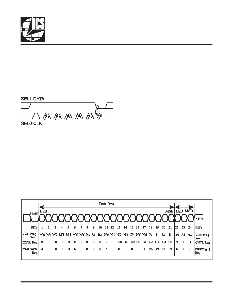
Serial Programming Architecture
The pins SEL0 and SEL1 perform the dual functions of
select-ing registers and serial programming. In serial
programming mode, SEL0 acts as a clock pin while SEL1
acts as the data pin. The ICS9161A-01 may not be serially
programmed when in power-down mode.
In order to program a particular register, an unlocking
sequence must occur.The unlocking sequence is detailed
in the following timing diagram:
Serial Data Register
The serial data is clocked into the serial data register in the
order described in Figure 1 below (Serial Data Timing).
The serial data is sent as follows: An individual data bit is
sampled on the rising edge of CLK.The complement of the
data bit must be sampled on the previous falling edge of
CLK. The setup and hold time requirements must be met
on both CLK edges. For specifics on timing, see the timing
diagrams on pages 10, 11 and 12.
The bits are shifted in this order: a start bit, 21 data bits,
3 address bits (which designate the desired register), and
a stop bit. A total of 24 bits must always be loaded into the
serial data register or an error is issued. Following the entry
of the last data bit, a stop bit or load command is issued
by bringing DATA high and toggling CLK high-to-low and
low-to-high. The unlocking mechanism then resets itself
following the load. Only after a time-out period are the
SEL0 and SEL1 pins allowed to return to a register
selection function.
Since the VCLK registers are selected by the SEL0 and
SEL1 pins, and since any change in their state may affect
the output frequency, new data input on the selection bits
is only permitted to pass through the decode logic after the
watchdog timer has timed out.This delay of SEL0 or SEL1
data permits a serial program cycle to occur without
affecting the current register selection.
The unlock sequence consists of at least five low-to-high
transitions of CLK while data is high, followed immediately
by a single low-to-high transition while data is low. Following
this unlock sequence, data can be loaded into the serial
data register.This programming must include the start bit,
shown in Figure 1.
Following any transition of CLK or DATA, the watchdog
timer is reset and begins counting. The watchdog timer
ensures that successive rising edges of CLK and DATA do
not violate the time-out specification of 2ms. If a time-out
occurs, the lock mechanism is reset and the data in the
serial data register is ignored.
Figure 1: Serial Data Timing
相关PDF资料 |
PDF描述 |
|---|---|
| ICS91730AMLF | IC CLOCK GENERATOR LOW EMI 8SOIC |
| ICS9173B-15CS08LF | IC PLL VIDEO GENLOCK 8SOIC |
| ICS9248BF-138LFT | IC FREQ GENERATOR/BUFFER 48-SSOP |
| ICS9250BF-12LF | IC FREQ TIMING GENERATOR 56-SSOP |
| ICS9250BF-28 | IC FREQ GENERATOR/BUFFER 56-SSOP |
相关代理商/技术参数 |
参数描述 |
|---|---|
| ICS9161-XXCN16 | 制造商:未知厂家 制造商全称:未知厂家 功能描述:Video/Graphics Clock Generator |
| ICS9161-XXCW16 | 制造商:未知厂家 制造商全称:未知厂家 功能描述:Video/Graphics Clock Generator |
| ICS9169A-70 | 制造商:IDT 制造商全称:Integrated Device Technology 功能描述:Frequency Generator for Workstation Systems |
| ICS9169AM-70 | 制造商:ICS 制造商全称:ICS 功能描述:Frequency Generator for Workstation Systems |
| ICS9169C-231 | 制造商:ICS 制造商全称:ICS 功能描述:Frequency Generator for Pentium Based Systems |
发布紧急采购,3分钟左右您将得到回复。