- 您现在的位置:买卖IC网 > PDF目录362809 > ICS9176-01 Low Skew Output Buffer PDF资料下载
参数资料
| 型号: | ICS9176-01 |
| 英文描述: | Low Skew Output Buffer |
| 中文描述: | 低偏移输出缓冲 |
| 文件页数: | 1/8页 |
| 文件大小: | 379K |
| 代理商: | ICS9176-01 |
Integrated
Circuit
Systems, Inc.
General Description
t
he
ICS9176-01
is designed specifically to support the tight
timing requirements of high-performance microprocessors
and chip sets. Because the jitter of the device is limited to
±250ps, the
ICS9176-01
is ideal for clocking Pentium
systems. The 10 high drive (40mA), low-skew (±250ps)
outputs make the
ICS9176-01
a perfect fit for PCI clocking
requirements.
Features
ICS9176-01
-01 is pin compatible with Triquint GA1086
±500ps skew (max) between input and outputs
±250ps skew (max) between outputs
10 symmetric, TLL-compatible outputs
28-pin PLCC or 28-pin wide SOIC surface mount
package
High drive, 40mA outputs
Power-down option
Output frequency range 20 MHz to 120 MHz
Input frequency range 20 MHz to 100 MHz
Ideal for PCI bus applications
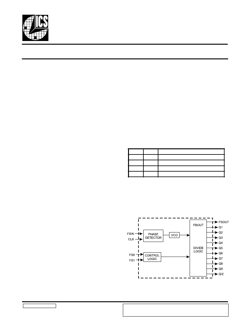
ICS9176-01
Block Diagram
ICS9176-01-01RevB061297P
Low Skew Output Buffer
Pentium is a trademark of Intel Corporation.
The
ICS9176-01
has 10 outputs synchronized in phase and
fre-quency to an input clock. The internal phase locked loop
(PLL) acts either as a 1X clock multiplier or a 1/2X clock
multiplier depending on the state of the input control pins T0
and T1. With metal mask options, any type of ratio between
the input clock and output clock can be achieved, including
2X.
The PLL maintains the phase and frequency relationship be-
tween the input clock and the outputs by externally feeding
back FBOUT to FBIN. Any change in the input will be tracked
by all 10 outputs. However, the change at the outputs will
happen smoothly so no glitches will be present on any driven
input. The PLL circuitry matches rising edges of the input
clock and the output clock. Since the input to FBIN skew is
guaran-teed to ±500ps, the part acts as a “zero delay” buffer.
The
ICS9176-01
has a total of eleven outputs. Of these,
FBOUT is dedicated as the feedback into the PLL and another,
Q/2, has an output frequency half that of the remaining nine.
These nine outputs can either be running at the same speed as
the input, or at half the frequency of the input. With Q/2 as the
feedback to FBIN, the nine ‘Q’ outputs will be running at twice
the input frequency in the normal divide-by-1 mode. In this
case, the output can go to 120 MHz with a 60 MHz input clock.
The maximum rise and fall time of an output is 1ns and each is
TTL-compatible with a 40mA symmetric drive.
The
ICS9176-01
is fabricated using CMOS technology which
results in much lower power consumption and cost compared
with the gallium arsenide based 1086E. The typical operating
current for the
ICS9176-01
is 60mA versus 115mA for the
GA1086E.
Functionality
FS1
0
0
1
1
FS0
0
1
0
1
DESCRIPTION
Power-down
Test Mode (PLL Off CLK=outputs)
Normal (PLL On)
Divide by 2 Mode
ICS reserves the right to make changes in the device data identified in this publication
without further notice. ICS advises its customers to obtain the latest version of all
device data to verify that any information being relied upon by the customer is current
and accurate.
相关PDF资料 |
PDF描述 |
|---|---|
| ICS9222-01 | Dual Memory Clock Generator |
| ICS9248-199 | Frequency Generator for SIS 735/740 with AMD K7 Processor |
| ICS9248YF-199-T | Frequency Generator for SIS 735/740 with AMD K7 Processor |
| ICS932S200 | Frequency Timing Generator for Dual Server/Workstation Systems |
| ICS932S200YF-T | Frequency Timing Generator for Dual Server/Workstation Systems |
相关代理商/技术参数 |
参数描述 |
|---|---|
| ICS9176-01CQ28 | 制造商:未知厂家 制造商全称:未知厂家 功能描述:CPU System Clock Generator |
| ICS9176CM-03 | 制造商:未知厂家 制造商全称:未知厂家 功能描述:CPU SYSTEM CLOCK GENERATOR|CMOS|SOP|28PIN|PLASTIC |
| ICS9176CQ-03 | 制造商:未知厂家 制造商全称:未知厂家 功能描述:CPU System Clock Generator |
| ICS9176M-01 | 制造商:ICS 制造商全称:ICS 功能描述:Low Skew Output Buffer |
| ICS9176Q-01 | 制造商:未知厂家 制造商全称:未知厂家 功能描述:CPU System Clock Generator |
发布紧急采购,3分钟左右您将得到回复。