- 您现在的位置:买卖IC网 > PDF目录67707 > ICS950410YF-T 300 MHz, PROC SPECIFIC CLOCK GENERATOR, PDSO48 PDF资料下载
参数资料
| 型号: | ICS950410YF-T |
| 元件分类: | 时钟产生/分配 |
| 英文描述: | 300 MHz, PROC SPECIFIC CLOCK GENERATOR, PDSO48 |
| 封装: | 0.300 INCH, MO-118, SSOP-48 |
| 文件页数: | 15/16页 |
| 文件大小: | 210K |
| 代理商: | ICS950410YF-T |
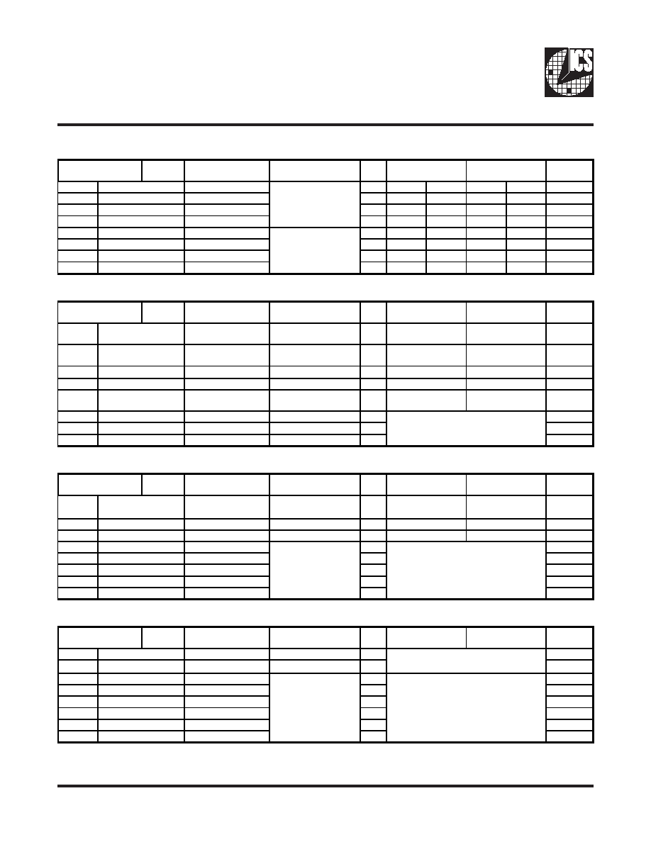
8
ICS950410
Preliminary Product Preview
0888A—04/22/05
I
2C Table: Skew Control Register
Bit 7
PCI/HTTSkw3
RW
0000:0
0100:150 1000:300 1100:450
1
Bit 6
PCI/HTTSkw2
RW
0001:N/A 0101:N/A 1001:N/A 1101:600
1
Bit 5
PCI/HTTSkw1
RW
0010:N/A 0110:N/A 1010:N/A 1110:750
0
Bit 4
PCI/HTTSkw0
RW
0011:N/A 0111:N/A 1011:N/A 1111:900
0
Bit 3
PCISkw3
RW
0000:0
0100:150 1000:300 1100:450
1
Bit 2
PCISkw2
RW
0001:N/A 0101:N/A 1001:N/A 1101:600
1
Bit 1
PCISkw1
RW
0010:N/A 0110:N/A 1010:N/A 1110:750
0
Bit 0
PCISkw0
RW
0011:N/A 0111:N/A 1011:N/A 1111:900
0
I
2C Table: WD Time Control & Async Frequency Selection Register
Bit 7
ASEL
Async Frequency
Select
RW
0
Bit 6
AEN
AGP/PCI/ Freq Source
Select
RW
1
Bit 5
REF1 Strength
REF1 strength control
RW
1
Bit 4
Reserved
RW
1
Bit 3
WDTCtrl
Watch Dog Time base
Control
RW
0
Bit 2
WD2
WD Timer Bit 2
RW
1
Bit 1
WD1
WD Timer Bit 1
RW
1
Bit 0
WD0
WD Timer Bit 0
RW
1
I
2C Table: VCO Control Select Bit & WD Timer Control Register
Bit 7
M/NEN
M/N Programming
Enable
RW
0
Bit 6
WDEN
Watchdog Enable
RW
0
Bit 5
WDStatus
WD Alarm Status
R
0
Bit 4
WD SF4
RW
0
Bit 3
WD SF3
RW
0
Bit 2
WD SF2
RW
0
Bit 1
WD SF1
RW
0
Bit 0
WD SF0
RW
0
I
2C Table: VCO Frequency Control Register
Bit 7
N Div8
N Divider Prog bit 8
RW
X
Bit 6
N Div9
N Divider Prog bit 9
RW
X
Bit 5
M Div5
RW
X
Bit 4
M Div4
RW
X
Bit 3
M Div3
RW
X
Bit 2
M Div2
RW
X
Bit 1
M Div1
RW
X
Bit 0
M Div0
RW
X
CPU-PCI/HTT 7 Step
Skew Control (ps)
CPU-PCI 7 Step Skew
Control (ps)
M Divider Programming
bits (5:0)
The decimal representation of M and N
Divier in Byte 11 and 12 will configure the
VCO frequency. Default at power up =
latch-in or Byte 0 Rom table.
VCO Frequency = 14.318 x [NDiv(9:0)+8]
/ [MDiv(5:0)+2]
The decimal representation of N Divider in
Byte 11 and 12
Type
0
1
-
PWD
Byte 11
Pin #
Name
Control Function
-
Normal
Alarm
-
Watch Dog Safe Freq
Programming bits
Writing to these bit will configure the safe
frequency as Byte0 bit (4:0).
-
Disable
Enable
-
Disable
Enable
1PWD
Byte 10
Pin #
Name
Control Function
Type
0
-
These bits represent X*290ms (or 1.16S)
the watchdog timer waits before it goes to
alarm mode. Default is 7 X 290ms = 2s.
-
--
-
290ms Base
1160ms Base
-
66MHz
75.4MHz
FIX PLL
CPU PLL
1x
2x
Type
0
1
PWD
Byte 9
Pin #
Name
Control Function
-
Type
0
1
PWD
Byte 8
Pin #
Name
Control Function
相关PDF资料 |
PDF描述 |
|---|---|
| ICS950602YFT | 200 MHz, PROC SPECIFIC CLOCK GENERATOR, PDSO48 |
| ICS950602YFLFT | 200 MHz, PROC SPECIFIC CLOCK GENERATOR, PDSO48 |
| ICS950806YGT | 200 MHz, PROC SPECIFIC CLOCK GENERATOR, PDSO56 |
| ICS950810YFT-LF | 200 MHz, PROC SPECIFIC CLOCK GENERATOR, PDSO56 |
| ICS950810YGT-LF | 200 MHz, PROC SPECIFIC CLOCK GENERATOR, PDSO56 |
相关代理商/技术参数 |
参数描述 |
|---|---|
| ICS950508 | 制造商:ICS 制造商全称:ICS 功能描述:Programmable Timing Control HubTM for PII/IIITTM |
| ICS950508YFLF-T | 制造商:ICS 制造商全称:ICS 功能描述:Programmable Timing Control HubTM for PII/IIITTM |
| ICS950602 | 制造商:ICS 制造商全称:ICS 功能描述:Programmable Timing Control Hub for PII/III |
| ICS950602CF | 功能描述:IC TIMING CTRL HUB P4 48-SSOP RoHS:否 类别:集成电路 (IC) >> 时钟/计时 - 专用 系列:TCH™ 标准包装:28 系列:- 类型:时钟/频率发生器 PLL:是 主要目的:Intel CPU 服务器 输入:时钟 输出:LVCMOS 电路数:1 比率 - 输入:输出:3:22 差分 - 输入:输出:无/是 频率 - 最大:400MHz 电源电压:3.135 V ~ 3.465 V 工作温度:0°C ~ 85°C 安装类型:表面贴装 封装/外壳:64-TFSOP (0.240",6.10mm 宽) 供应商设备封装:64-TSSOP 包装:管件 |
| ICS950602CFLF | 功能描述:IC TIMING CTRL HUB P4 48-SSOP RoHS:是 类别:集成电路 (IC) >> 时钟/计时 - 专用 系列:TCH™ 标准包装:28 系列:- 类型:时钟/频率发生器 PLL:是 主要目的:Intel CPU 服务器 输入:时钟 输出:LVCMOS 电路数:1 比率 - 输入:输出:3:22 差分 - 输入:输出:无/是 频率 - 最大:400MHz 电源电压:3.135 V ~ 3.465 V 工作温度:0°C ~ 85°C 安装类型:表面贴装 封装/外壳:64-TFSOP (0.240",6.10mm 宽) 供应商设备封装:64-TSSOP 包装:管件 |
发布紧急采购,3分钟左右您将得到回复。