- 您现在的位置:买卖IC网 > PDF目录362809 > ICS952011YFT Programmable Timing Control Hub for P4 processor PDF资料下载
参数资料
| 型号: | ICS952011YFT |
| 英文描述: | Programmable Timing Control Hub for P4 processor |
| 中文描述: | 可编程定时控制中心的P4处理器 |
| 文件页数: | 3/25页 |
| 文件大小: | 183K |
| 代理商: | ICS952011YFT |
3
Integrated
Circuit
Systems, Inc.
ICS952011
0721A—07/29/03
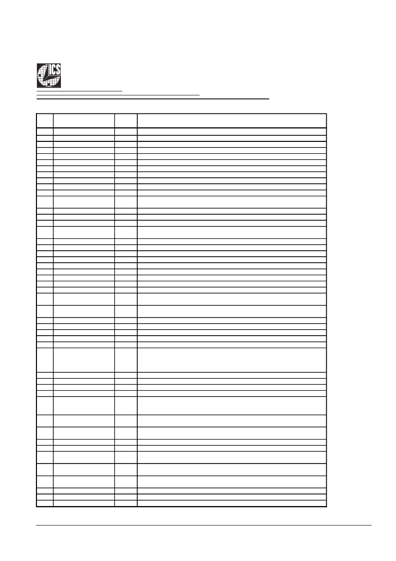
Pin Description
PIN
#
1
VDDREF
2
**FS0/REF0
3
**FS1/REF1
4
**FS2/REF2
5
GNDREF
6
X1
7
X2
8
GNDZ
9
ZCLK0
10
ZCLK1
11
VDDZ
PIN
NAME
PIN
TYPE
PWR
I/O
I/O
I/O
PWR
IN
OUT
PWR
OUT
OUT
PWR
Ref, XTAL power supply, nominal 3.3V
Frequency select latch input pin / 14.318 MHz reference clock.
Frequency select latch input pin / 14.318 MHz reference clock.
Frequency select latch input pin / 14.318 MHz reference clock.
Ground pin for the REF outputs.
Crystal input, Nominally 14.318MHz.
Crystal output, Nominally 14.318MHz
Ground pin for the ZCLK outputs
3.3V Hyperzip clock output.
3.3V Hyperzip clock output.
Power supply for ZCLK clocks, nominal 3.3V
Stops all PCICLKs besides the PCICLK_F clocks at logic 0 level, when input low. This
input is activated by the MODE selection pin / PCI clock output.
Power supply for PCI clocks, nominal 3.3V
Frequency select latch input pin / 3.3V PCI free running clock output.
Frequency select latch input pin / 3.3V PCI free running clock output.
12
*(PCI_STOP#)PCICLK6
I/O
13
14
15
VDDPCI
**FS3/PCICLK_F0
**FS4/PCICLK_F1
PWR
I/O
I/O
16
*MODE0/PCICLK0
PCICLK1
GNDPCI
VDDPCI
PCICLK2
PCICLK3
PCICLK4
PCICLK5
GNDPCI
GND48
I/O
Function select latch input pin, 1=Desktop Mode, 0=Mobile Mode / PCI clock output.
17
18
19
20
21
22
23
24
25
OUT
PWR
PWR
OUT
OUT
OUT
OUT
PWR
PWR
PCI clock output.
Ground pin for the PCI outputs
Power supply for PCI clocks, nominal 3.3V
PCI clock output.
PCI clock output.
PCI clock output.
PCI clock output.
Ground pin for the PCI outputs
Ground pin for the 48MHz outputs
24MHz/48MHz clock output / Latched select input for 24/48MHz output. 0=48MHz, 1 =
24MHz.
12MHz/48MHz clock output / Latched select input for 24/48MHz output. 0=48MHz, 1 =
12MHz.
Power pin for the 48MHz output.3.3V
Power supply for AGP clocks, nominal 3.3V
AGP clock output
AGP clock output
Ground pin for the AGP outputs
26
24_48MHz/SEL24_48#*~
I/O
27
12_48MHz/SEL12_48#**
I/O
28
29
30
31
32
VDD48
VDDAGP
AGPCLK1
AGPCLK0
GNDAGP
PWR
PWR
OUT
OUT
PWR
33
Vtt_PwrGd/PD#(CPUSTOP
#)*
I/O
This 3.3V LVTTL input is a level sensitive strobe used to determine when latch inputs
are valid and are ready to be sampled. This is an active high input. Active low Power
Down input or active low CPU_STOP depend on B24b3 IIC selection. Default is PD#.
34
35
36
37
SDATA
SCLK
VDDA
GND
I/O
IN
PWR
PWR
Data pin for I2C circuitry 5V tolerant
Clock pin of I2C circuitry 5V tolerant
3.3V power for the PLL core.
Ground pin.
This pin establishes the reference current for the differential current-mode output pairs.
This pin requires a fixed precision resistor tied to ground in order to establish the
appropriate current. 475 ohms is the standard value.
"Complimentary" clocks of differential pair CPU outputs. These are current mode
outputs. External resistors are required for voltage bias.
"True" clocks of differential pair CPU outputs. These are current mode outputs.
External resistors are required for voltage bias.
Ground pin for the CPU outputs
Supply for CPU clocks, 3.3V nominal
"Complimentary" clocks of differential pair CPU outputs. These are current mode
outputs. External resistors are required for voltage bias.
"True" clocks of differential pair CPU outputs. These are current mode outputs.
External resistors are required for voltage bias.
Active low CPU_STOP or Active low Power Down input depend on B24b3 IIC selection.
Default is CPU_STOP#.
Ground pin.
SDRAM seed clock output for external buffer
Supply for SDRAM clocks, nominal 3.3V.
* Internal Pull-Up Resistor ** Internal Pull-Down Resistor
38
IREF
OUT
39
CPUCLKC0
OUT
40
CPUCLKT0
OUT
41
42
GNDCPU
VDDCPU
PWR
PWR
43
CPUCLKC1
OUT
44
CPUCLKT1
OUT
45
CPU_STOP#(PD#)*
IN
46
47
48
GND
SDRAM_OUT
VDDSDR
PWR
OUT
PWR
DESCRIPTION
相关PDF资料 |
PDF描述 |
|---|---|
| ICS952623 | Programmable Timing Control Hub for Next Gen P4 processor |
| ICS952623YFT | Programmable Timing Control Hub for Next Gen P4 processor |
| ICS952623YGT | Programmable Timing Control Hub for Next Gen P4 processor |
| ICS952623 | Programmable Timing Control Hub for Next Gen P4 processor |
| ICS952623YFT | Programmable Timing Control Hub for Next Gen P4 processor |
相关代理商/技术参数 |
参数描述 |
|---|---|
| ICS952101CF | 功能描述:IC FREQ GENERATOR 56-SSOP RoHS:否 类别:集成电路 (IC) >> 时钟/计时 - 专用 系列:- 标准包装:1,500 系列:- 类型:时钟缓冲器/驱动器 PLL:是 主要目的:- 输入:- 输出:- 电路数:- 比率 - 输入:输出:- 差分 - 输入:输出:- 频率 - 最大:- 电源电压:3.3V 工作温度:0°C ~ 70°C 安装类型:表面贴装 封装/外壳:28-SSOP(0.209",5.30mm 宽) 供应商设备封装:28-SSOP 包装:带卷 (TR) 其它名称:93786AFT |
| ICS952101CFLF | 功能描述:IC FREQ GENERATOR 56-SSOP RoHS:是 类别:集成电路 (IC) >> 时钟/计时 - 专用 系列:- 标准包装:1,500 系列:- 类型:时钟缓冲器/驱动器 PLL:是 主要目的:- 输入:- 输出:- 电路数:- 比率 - 输入:输出:- 差分 - 输入:输出:- 频率 - 最大:- 电源电压:3.3V 工作温度:0°C ~ 70°C 安装类型:表面贴装 封装/外壳:28-SSOP(0.209",5.30mm 宽) 供应商设备封装:28-SSOP 包装:带卷 (TR) 其它名称:93786AFT |
| ICS952101CFLFT | 功能描述:IC FREQ GENERATOR 56-SSOP RoHS:是 类别:集成电路 (IC) >> 时钟/计时 - 专用 系列:- 标准包装:1,500 系列:- 类型:时钟缓冲器/驱动器 PLL:是 主要目的:- 输入:- 输出:- 电路数:- 比率 - 输入:输出:- 差分 - 输入:输出:- 频率 - 最大:- 电源电压:3.3V 工作温度:0°C ~ 70°C 安装类型:表面贴装 封装/外壳:28-SSOP(0.209",5.30mm 宽) 供应商设备封装:28-SSOP 包装:带卷 (TR) 其它名称:93786AFT |
| ICS952101CFT | 功能描述:IC FREQ GENERATOR 56-SSOP RoHS:否 类别:集成电路 (IC) >> 时钟/计时 - 专用 系列:- 标准包装:1,500 系列:- 类型:时钟缓冲器/驱动器 PLL:是 主要目的:- 输入:- 输出:- 电路数:- 比率 - 输入:输出:- 差分 - 输入:输出:- 频率 - 最大:- 电源电压:3.3V 工作温度:0°C ~ 70°C 安装类型:表面贴装 封装/外壳:28-SSOP(0.209",5.30mm 宽) 供应商设备封装:28-SSOP 包装:带卷 (TR) 其它名称:93786AFT |
| ICS952301 | 制造商:ICS 制造商全称:ICS 功能描述:Frequency Timing Generator for Transmeta Systems |
发布紧急采购,3分钟左右您将得到回复。