- 您现在的位置:买卖IC网 > PDF目录67710 > ICSLV810FI (INTEGRATED DEVICE TECHNOLOGY INC) 810 SERIES, LOW SKEW CLOCK DRIVER, 10 TRUE OUTPUT(S), 0 INVERTED OUTPUT(S), PDSO20 PDF资料下载
参数资料
| 型号: | ICSLV810FI |
| 厂商: | INTEGRATED DEVICE TECHNOLOGY INC |
| 元件分类: | 时钟及定时 |
| 英文描述: | 810 SERIES, LOW SKEW CLOCK DRIVER, 10 TRUE OUTPUT(S), 0 INVERTED OUTPUT(S), PDSO20 |
| 封装: | 0.209 INCH, SSOP-20 |
| 文件页数: | 8/14页 |
| 文件大小: | 299K |
| 代理商: | ICSLV810FI |
ICSLV810
BUFFER/CLOCK DRIVER
FAN OUT BUFFER
IDT / ICS BUFFER/CLOCK DRIVER
3
ICSLV810
REV F 101305
External Components
The ICSLV810 requires a minimum number of external
components for proper operation.
Decoupling Capacitors
Decoupling capacitors of 0.01F must be connected
between VDD and GND, as close to these pins as possible.
For optimum device performance, the decoupling capacitors
should be mounted on the component side of the PCB.
Avoid the use of vias in the decoupling circuit.
Series Termination Resistor
When the PCB trace between the clock outputs and the
loads are over 1 inch, series termination should be used. To
series terminate a 50
trace (a commonly used trace
impedance) place a 33
resistor in series with the clock
line, as close to the clock output pin as possible. The
nominal impedance of the clock output is 20
.
PCB Layout Recommendations
For optimum device performance and lowest output phase
noise, the following guidelines should be observed.
1) The 0.01F decoupling capacitors should be mounted on
the component side of the board as close to the VDD pins
as possible. No vias should be used between the
decoupling capacitors and VDD pins. The PCB trace to VDD
pin should be kept as short as possible, as should the PCB
trace to the ground via.
2) To minimize EMI the 33
series termination resistor, if
needed, should be placed close to the clock output.
Absolute Maximum Ratings
Stresses above the ratings listed below can cause permanent damage to the ICSLV810. These ratings, which are
standard values for ICS commercially rated parts, are stress ratings only. Functional operation of the device at
these or any other conditions above those indicated in the operational sections of the specifications is not implied.
Exposure to absolute maximum rating conditions for extended periods can affect product reliability. Electrical
parameters are guaranteed only over the recommended operating temperature range.
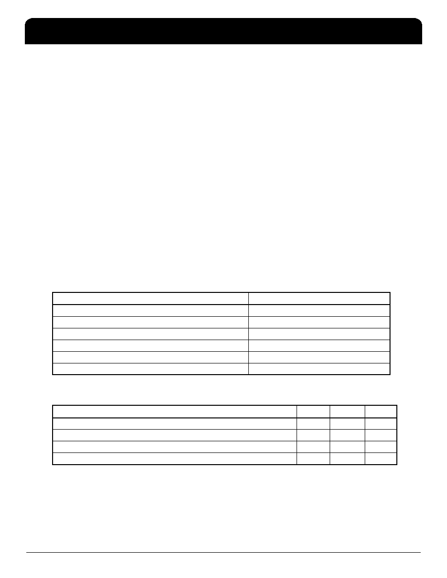
Recommended Operation Conditions
Item
Rating
Supply Voltage, VDD MAX
7 V
All Inputs and Outputs
-0.5 V to VDDA + 1.2 V
Ambient Operating Temperature
-40 to +85
°C
Storage Temperature
-65 to +150
°C
Junction Temperature
125
°C
Soldering Temperature
260
°C
Parameter
Min.
Typ.
Max.
Units
Ambient Operating Temperature
-40
+85
°C
Power Supply Voltage (measured with respect to GND), VDDA
1.425
2.625
V
Power Supply Voltage (measured with respect to GND), VDDB
1.425
2.625
V
Power Supply Voltage (measured with respect to GND), VDDC
1.425
2.625
V
相关PDF资料 |
PDF描述 |
|---|---|
| ICSLV810FIT | 810 SERIES, LOW SKEW CLOCK DRIVER, 10 TRUE OUTPUT(S), 0 INVERTED OUTPUT(S), PDSO20 |
| ICSLV810SIT | 810 SERIES, LOW SKEW CLOCK DRIVER, 10 TRUE OUTPUT(S), 0 INVERTED OUTPUT(S), PDSO20 |
| ICSLV810SILF | 810 SERIES, LOW SKEW CLOCK DRIVER, 10 TRUE OUTPUT(S), 0 INVERTED OUTPUT(S), PDSO20 |
| ICSLV810SI | 810 SERIES, LOW SKEW CLOCK DRIVER, 10 TRUE OUTPUT(S), 0 INVERTED OUTPUT(S), PDSO20 |
| ICSS98UAE877AHLFIT | 98UAE SERIES, PLL BASED CLOCK DRIVER, 10 TRUE OUTPUT(S), 0 INVERTED OUTPUT(S), PBGA52 |
相关代理商/技术参数 |
参数描述 |
|---|---|
| ICSLV810FILF | 制造商:ICS 制造商全称:ICS 功能描述:Buffer/Clock Driver |
| ICSLV810FILFT | 制造商:ICS 制造商全称:ICS 功能描述:Buffer/Clock Driver |
| ICSLV810FIT | 制造商:ICS 制造商全称:ICS 功能描述:Buffer/Clock Driver |
| ICSLV810RI | 制造商:ICS 制造商全称:ICS 功能描述:Buffer/Clock Driver |
| ICSLV810RILF | 制造商:ICS 制造商全称:ICS 功能描述:Buffer/Clock Driver |
发布紧急采购,3分钟左右您将得到回复。