- 您现在的位置:买卖IC网 > PDF目录65576 > IDT5993A-2Q8 (INTEGRATED DEVICE TECHNOLOGY INC) PLL BASED CLOCK DRIVER, 8 TRUE OUTPUT(S), 0 INVERTED OUTPUT(S), PDSO28 PDF资料下载
参数资料
| 型号: | IDT5993A-2Q8 |
| 厂商: | INTEGRATED DEVICE TECHNOLOGY INC |
| 元件分类: | 时钟及定时 |
| 英文描述: | PLL BASED CLOCK DRIVER, 8 TRUE OUTPUT(S), 0 INVERTED OUTPUT(S), PDSO28 |
| 封装: | QSOP-28 |
| 文件页数: | 3/8页 |
| 文件大小: | 65K |
| 代理商: | IDT5993A-2Q8 |
3
COMMERCIALANDINDUSTRIALTEMPERATURERANGES
IDT5993A
PROGRAMMABLESKEWPLLCLOCKDRIVERTURBOCLOCK
EXTERNALFEEDBACK
By providing external feedback, the IDT5993A gives users flexibility
with regard to skew adjustment. The FB signal is compared with the
input REF signal at the phase detector in order to drive the VCO. Phase
differences cause the VCO of the PLL to adjust upwards or downwards
accordingly.
NOTES:
1. The device may be operated outside recommended frequency ranges without damage, but functional operation is not guaranteed. Selecting the appropriate FS value based on
input frequency range allows the PLL to operate in its ‘sweet spot’ where jitter is lowest.
2. The level to be set on FS is determined by the nominal operating frequency of the VCO and Time Unit Generator. The VCO frequency always appears at 1Q1:0, 2Q1:0, and the
higher outputs when they are operated in their undivided modes. The frequency appearing at the REF and FB inputs will be the same as the VCO when the output connected
to FB is undivided. The frequency of the REF and FB inputs will be 1/2 or 1/4 the VCO frequency when the part is configured for a frequency multiplication by using a divided
output as the FB input.
3. Skew adjustment range assumes that a zero skew output is used for feedback. If a skewed Q output is used for feedback, then adjustment range will be greater. For example
if a 4tU skewed output is used for feedback, all other outputs will be skewed –4tU in addition to whatever skew value is programmed for those outputs. ‘Max adjustment’ range
applies to output pairs 3 and 4 where ± 6tU skew adjustment is possible and at the lowest FNOM value.
An internal loop filter moderates the response of the VCO to the
phase detector. The loop filter transfer function has been chosen to
provide minimal jitter (or frequency variation) while still providing accu-
rate responses to input frequency changes.
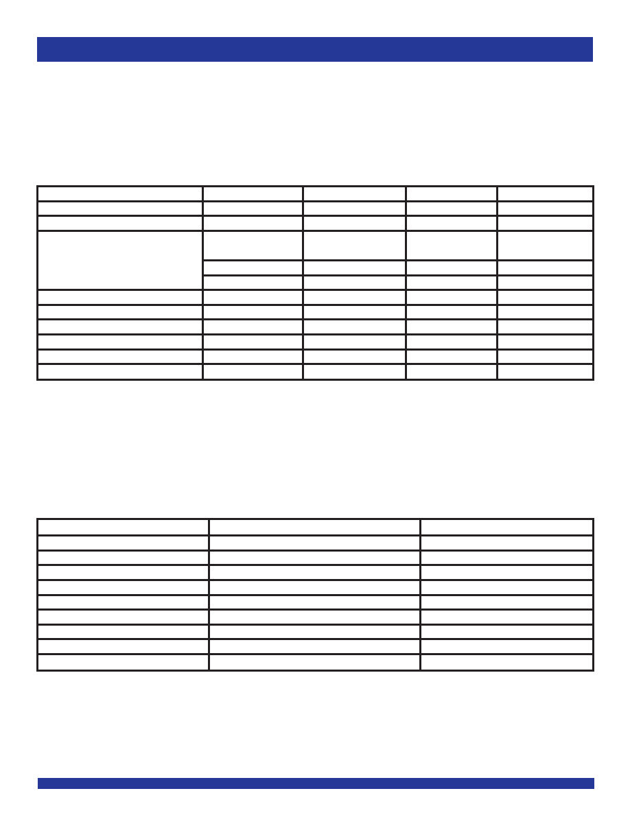
FS = LOW
FS = MID
FS = HIGH
Comments
TimingUnitCalculation(tU)
1/(44 x FNOM)
1/(26 x FNOM)
1/(16 x FNOM)
VCO Frequency Range (FNOM)(1,2)
15 to 35MHz
25 to 60MHz
40 to 100 MHz
SkewAdjustmentRange(3)
Max Adjustment:
±9.09ns
±9.23ns
±9.38ns
ns
±49°
±83°
±135°
PhaseDegrees
±14%
±23%
±37%
% of Cycle Time
Example 1, FNOM = 15MHz
tU = 1.52ns
—
Example 2, FNOM = 25MHz
tU = 0.91ns
tU = 1.54ns
—
Example 3, FNOM = 30MHz
tU = 0.76ns
tU = 1.28ns
—
Example 4, FNOM = 40MHz
—
tU = 0.96ns
tU = 1.56ns
Example 5, FNOM = 50MHz
—
tU = 0.77ns
tU = 1.25ns
Example 6, FNOM = 80MHz
—
tU = 0.78ns
PLL PROGRAMMABLE SKEW RANGE AND RESOLUTION TABLE
CONTROL SUMMARY TABLE FOR FEEDBACK SIGNALS
nF1:0
Skew (Pair #1, #2)
Skew (Pair #3)
LL(1)
–4tU
Divide by 2
LM
–3tU
–6tU
LH
–2tU
–4tU
ML
–1tU
–2tU
M M
Zero Skew
MH
1tU
2tU
HL
2tU
4tU
HM
3tU
6tU
HH
4tU
Divide by 4
NOTE:
1. LL disables outputs if TEST = MID and GND/sOE = HIGH.
相关PDF资料 |
PDF描述 |
|---|---|
| IDT5993A-7QI8 | PLL BASED CLOCK DRIVER, 8 TRUE OUTPUT(S), 0 INVERTED OUTPUT(S), PDSO28 |
| IDT5T9070PAGI | 5T SERIES, LOW SKEW CLOCK DRIVER, 10 TRUE OUTPUT(S), 0 INVERTED OUTPUT(S), PDSO48 |
| IDT5T9950APFGI | 5T SERIES, PLL BASED CLOCK DRIVER, 8 TRUE OUTPUT(S), 0 INVERTED OUTPUT(S), PQFP32 |
| IDT5T9950APFGI8 | 5T SERIES, PLL BASED CLOCK DRIVER, 8 TRUE OUTPUT(S), 0 INVERTED OUTPUT(S), PQFP32 |
| IDT5T9950PFI | 5T SERIES, PLL BASED CLOCK DRIVER, 8 TRUE OUTPUT(S), 0 INVERTED OUTPUT(S), PQFP32 |
相关代理商/技术参数 |
参数描述 |
|---|---|
| IDT5P30017NDGI | 制造商:Integrated Device Technology Inc 功能描述:IC CLOCK GENERATOR 28QFN |
| IDT5P30017NDGI8 | 制造商:Integrated Device Technology Inc 功能描述:IC CLOCK GENERATOR 28QFN |
| IDT5P30018NBG8 | 制造商:Integrated Device Technology Inc 功能描述:IC CLOCK GENERATOR 28QFN |
| IDT5P49EE502NDGI | 制造商:Integrated Device Technology Inc 功能描述:IC CLOCK GENERATOR 20QFN |
| IDT5P49EE502NDGI8 | 制造商:Integrated Device Technology Inc 功能描述:IC CLOCK GENERATOR 28QFN |
发布紧急采购,3分钟左右您将得到回复。