- 您现在的位置:买卖IC网 > PDF目录65576 > IDT5T9950APFGI8 (INTEGRATED DEVICE TECHNOLOGY INC) 5T SERIES, PLL BASED CLOCK DRIVER, 8 TRUE OUTPUT(S), 0 INVERTED OUTPUT(S), PQFP32 PDF资料下载
参数资料
| 型号: | IDT5T9950APFGI8 |
| 厂商: | INTEGRATED DEVICE TECHNOLOGY INC |
| 元件分类: | 时钟及定时 |
| 英文描述: | 5T SERIES, PLL BASED CLOCK DRIVER, 8 TRUE OUTPUT(S), 0 INVERTED OUTPUT(S), PQFP32 |
| 封装: | LEAD FREE, TQFP-32 |
| 文件页数: | 3/9页 |
| 文件大小: | 81K |
| 代理商: | IDT5T9950APFGI8 |
3
INDUSTRIALTEMPERATURERANGE
IDT5T9950/A
2.5V PROGRAMMABLE SKEW PLL CLOCK DRIVER TURBOCLOCK II JR.
Output skew with respect to the REF input is adjustable to compensate
for PCB trace delays, backplane propagation delays or to accommodate
requirements for special timing relationships between clocked compo-
nents. Skew is selectable as a multiple of a time unit (tU) which ranges
from 782ps to 1.5625ns for Standard version and 6.25ps to 1.3ns for A
version (see Programmable Skew Range and Resolution Table). There
are nine skew configurations available for each output pair. These con-
figurations are chosen by the nF1:0 control pins. In order to minimize the
number of control pins, 3-level inputs (HIGH-MID-LOW) are used, they
are intended for but not restricted to hard-wiring. Undriven 3-level in-
puts default to the MID level. Where programmable skew is not a re-
quirement, the control pins can be left open for the zero skew default
setting. The Control Summary Table shows how to select specific skew
taps by using the nF1:0 control pins.
PROGRAMMABLESKEW
EXTERNALFEEDBACK
By providing external feedback, the IDT5T9950 gives users flexibility
with regard to skew adjustment. The FB signal is compared with the
input REF signal at the phase detector in order to drive the VCO. Phase
differences cause the VCO of the PLL to adjust upwards or downwards
accordingly.
NOTES:
1. The device may be operated outside recommended frequency ranges without damage, but functional operation is not guaranteed.
2. The level to be set on FS is determined by the nominal operating frequency of the VCO and Time Unit Generator. The VCO frequency always appears at 1Q1:0, 2Q1:0, and
the higher outputs when they are operated in their undivided modes. The frequency appearing at the REF and FB inputs will be the same as the VCO when the output connected
to FB is undivided. The frequency of the REF and FB inputs will be 1/2 or 1/4 the VCO frequency when the part is configured for frequency multiplication by using a divided
output as the FB input.
3. Skew adjustment range assumes that a zero skew output is used for feedback. If a skewed Q output is used for feedback, then adjustment range will be greater. For example
if a 4tU skewed output is used for feedback, all other outputs will be skewed –4tU in addition to whatever skew value is programmed for those outputs. ‘Max adjustment’ range
applies to output pairs 3 and 4 where ± 6tU skew adjustment is possible and at the lowest FNOM value.
An internal loop filter moderates the response of the VCO to the
phase detector. The loop filter transfer function has been chosen to
provide minimal jitter (or frequency variation) while still providing accu-
rate responses to input frequency changes.
IDT5T9950
IDT5T9950A
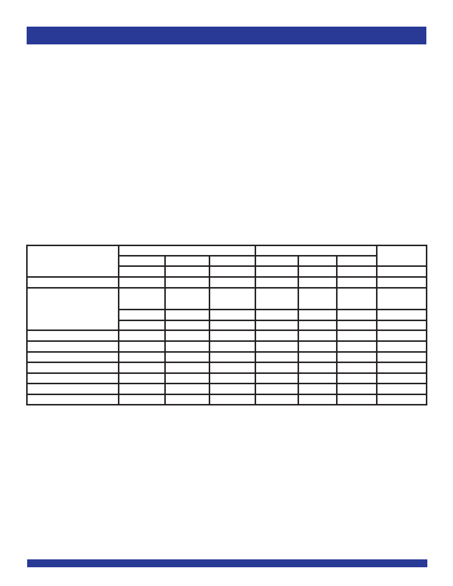
FS = LOW
FS = MID
FS = HIGH
FS = LOW
FS = MID
FS = HIGH
Comments
Timing Unit Calculation (tU)
1/(32 x FNOM)
1/(16 x FNOM)
1/(8 x FNOM)
1/(32 x FNOM) 1/(16 x FNOM)
1/(8 x FNOM)
VCO Frequency Range (FNOM)(1,2)
24 to 40MHz
40 to 80MHz
80 to 160MHz
24 to 50MHz
48 to 100MHz
96 to 200MHz
Skew Adjustment Range(3)
Max Adjustment:
±7.8125ns
±9.375ns
±7.8125ns
ns
±67.5°
±135°
±270°
±67.5°
±135°
±270°
Phase Degrees
±18.75%
±37.5%
±75%
±18.75%
±37.5%
±75%
% of Cycle Time
Example 1, FNOM = 25MHz
tU = 1.25ns
—
tU = 1.25ns
—
Example 2, FNOM = 37.5MHz
tU = 0.833ns
—
tU = 0.833ns
—
Example 3, FNOM = 50MHz
—
tU = 1.25ns
—
tU = 0.625ns
tU = 1.25ns
—
Example 4, FNOM = 75MHz
—
tU = 0.833ns
—
tU = 0.833ns
—
Example 5, FNOM = 100MHz
—
tU = 1.25ns
—
tU = 0.625ns
tU = 1.25ns
Example 6, FNOM = 150MHz
—
tU = 0.833ns
—
tU = 0.833ns
Example 7, FNOM = 200MHz
—
tU = 0.625ns
PROGRAMMABLE SKEW RANGE AND RESOLUTION TABLE
相关PDF资料 |
PDF描述 |
|---|---|
| IDT5T9950PFI | 5T SERIES, PLL BASED CLOCK DRIVER, 8 TRUE OUTPUT(S), 0 INVERTED OUTPUT(S), PQFP32 |
| IDT5T9950PFI8 | 5T SERIES, PLL BASED CLOCK DRIVER, 8 TRUE OUTPUT(S), 0 INVERTED OUTPUT(S), PQFP32 |
| IDT5T995PFGI | 5T SERIES, PLL BASED CLOCK DRIVER, 8 TRUE OUTPUT(S), 0 INVERTED OUTPUT(S), PQFP44 |
| IDT5T995APFI | 5T SERIES, PLL BASED CLOCK DRIVER, 8 TRUE OUTPUT(S), 0 INVERTED OUTPUT(S), PQFP44 |
| IDT5V2305NRGI8 | 5V SERIES, LOW SKEW CLOCK DRIVER, 5 TRUE OUTPUT(S), 0 INVERTED OUTPUT(S), PQCC16 |
相关代理商/技术参数 |
参数描述 |
|---|---|
| IDT5T9950PFGI | 功能描述:IC CLK BUFFER/DVR 1:10 32TQFP RoHS:是 类别:集成电路 (IC) >> 时钟/计时 - 时钟发生器,PLL,频率合成器 系列:TurboClock™ II JR 标准包装:2,000 系列:- 类型:PLL 频率合成器 PLL:是 输入:晶体 输出:时钟 电路数:1 比率 - 输入:输出:1:1 差分 - 输入:输出:无/无 频率 - 最大:1GHz 除法器/乘法器:是/无 电源电压:4.5 V ~ 5.5 V 工作温度:-20°C ~ 85°C 安装类型:表面贴装 封装/外壳:16-LSSOP(0.175",4.40mm 宽) 供应商设备封装:16-SSOP 包装:带卷 (TR) 其它名称:NJW1504V-TE1-NDNJW1504V-TE1TR |
| IDT5T9950PFGI8 | 功能描述:IC CLK BUFFER/DVR 1:10 32TQFP RoHS:是 类别:集成电路 (IC) >> 时钟/计时 - 时钟发生器,PLL,频率合成器 系列:TurboClock™ II JR 标准包装:1,000 系列:- 类型:时钟/频率合成器,扇出分配 PLL:- 输入:- 输出:- 电路数:- 比率 - 输入:输出:- 差分 - 输入:输出:- 频率 - 最大:- 除法器/乘法器:- 电源电压:- 工作温度:- 安装类型:表面贴装 封装/外壳:56-VFQFN 裸露焊盘 供应商设备封装:56-VFQFP-EP(8x8) 包装:带卷 (TR) 其它名称:844S012AKI-01LFT |
| IDT5T9955BFGI | 功能描述:IC CLK DRIVER DUAL PLL 96-FBGA RoHS:是 类别:集成电路 (IC) >> 时钟/计时 - 时钟发生器,PLL,频率合成器 系列:TurboClock™ W 标准包装:27 系列:Precision Edge® 类型:频率合成器 PLL:是 输入:PECL,晶体 输出:PECL 电路数:1 比率 - 输入:输出:1:1 差分 - 输入:输出:无/是 频率 - 最大:800MHz 除法器/乘法器:是/无 电源电压:3.135 V ~ 5.25 V 工作温度:0°C ~ 85°C 安装类型:表面贴装 封装/外壳:28-SOIC(0.295",7.50mm 宽) 供应商设备封装:28-SOIC 包装:管件 |
| IDT5T9955BFGI8 | 功能描述:IC CLK DRIVER DUAL PLL 96-FBGA RoHS:是 类别:集成电路 (IC) >> 时钟/计时 - 时钟发生器,PLL,频率合成器 系列:TurboClock™ W 标准包装:27 系列:Precision Edge® 类型:频率合成器 PLL:是 输入:PECL,晶体 输出:PECL 电路数:1 比率 - 输入:输出:1:1 差分 - 输入:输出:无/是 频率 - 最大:800MHz 除法器/乘法器:是/无 电源电压:3.135 V ~ 5.25 V 工作温度:0°C ~ 85°C 安装类型:表面贴装 封装/外壳:28-SOIC(0.295",7.50mm 宽) 供应商设备封装:28-SOIC 包装:管件 |
| IDT5T995APPGI | 功能描述:IC CLK DRIVER 2.5V PLL 44-TQFP RoHS:是 类别:集成电路 (IC) >> 时钟/计时 - 时钟发生器,PLL,频率合成器 系列:TurboClock™ II 标准包装:1,000 系列:- 类型:时钟/频率合成器,扇出分配 PLL:- 输入:- 输出:- 电路数:- 比率 - 输入:输出:- 差分 - 输入:输出:- 频率 - 最大:- 除法器/乘法器:- 电源电压:- 工作温度:- 安装类型:表面贴装 封装/外壳:56-VFQFN 裸露焊盘 供应商设备封装:56-VFQFP-EP(8x8) 包装:带卷 (TR) 其它名称:844S012AKI-01LFT |
发布紧急采购,3分钟左右您将得到回复。