- 您现在的位置:买卖IC网 > PDF目录67114 > IDT5T995APF (INTEGRATED DEVICE TECHNOLOGY INC) PLL BASED CLOCK DRIVER, 8 TRUE OUTPUT(S), 0 INVERTED OUTPUT(S), PQFP44 PDF资料下载
参数资料
| 型号: | IDT5T995APF |
| 厂商: | INTEGRATED DEVICE TECHNOLOGY INC |
| 元件分类: | 时钟及定时 |
| 英文描述: | PLL BASED CLOCK DRIVER, 8 TRUE OUTPUT(S), 0 INVERTED OUTPUT(S), PQFP44 |
| 封装: | TQFP-44 |
| 文件页数: | 8/10页 |
| 文件大小: | 197K |
| 代理商: | IDT5T995APF |
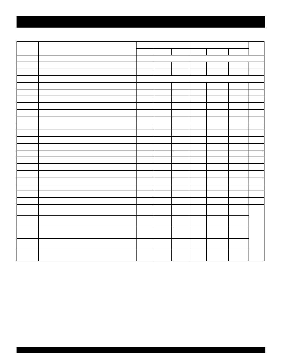
7
INDUSTRIALTEMPERATURERANGE
IDT5T995/A
2.5V PROGRAMMABLE SKEW PLL CLOCK DRIVER TURBOCLOCK II
SWITCHING CHARACTERISTICS OVER OPERATING RANGE
5T995
5T995A
Symbol
Parameter
Min.
Typ.
Max.
Min.
Typ.
Max.
Unit
FNOM
VCO Frequency Range
See Programmable Skew Range and Resolution Table
tRPWH
REF Pulse Width HIGH (10)
2—
—
2
—
ns
tRPWL
REF Pulse Width LOW (10)
2—
—
2
—
ns
tU
Programmable Skew Time Unit
See Control Summary Table
tSKEWPR
Zero Output Matched-Pair Skew (xQ0, xQ1) (1,2)
—
50
185
—
50
185
ps
tSKEW0
Zero Output Skew (All Outputs) (3)
—
0.1
0.25
—
0.1
0.25
ns
tSKEW1
Output Skew (Rise-Rise, Fall-Fall, Same Class Outputs) (4)
—
0.1
0.25
—
0.1
0.25
ns
tSKEW2
Output Skew (Rise-Fall, Nominal-Inverted, Divided-Divided) (4)
—
0.2
0.5
—
0.2
0.5
ns
tSKEW3
Output Skew (Rise-Rise, Fall-Fall, Different Class Outputs) (4)
—
0.15
0.5
—
0.15
0.5
ns
tSKEW4
Output Skew (Rise-Fall, Nominal-Divided, Divided-Inverted) (1)
—
0.3
0.9
—
0.3
0.9
ns
tDEV
Device-to-Device Skew (1,5)
—
0.75
—
0.75
ns
t(
φ)1-3
Static Phase Offset (FS = L, M, H, FB Divide-by-n = 1, 2, 3) (7)
0.3
—
0.3
0.25
—
0.25
ns
t(
φ)H
Static Phase Offset (FS = H)
0.5
—
0.5
0.25
—
0.25
ns
t(
φ)M
Static Phase Offset (FS = M)
0.7
—
0.7
0.5
—
0.5
ns
t(
φ)L1-6
Static Phase Offset (FS = L, FB Divide-by-n = 1, 2, 3, 4, 5, 6)
0.7
—
0.7
—
0.7
ns
t(
φ)L8-12
Static Phase Offset (FS = L, FB Divide-by-n = 8, 10, 12)
1—
1
1—
1
ns
tODCV
Output Duty Cycle Variation from 50%
1—
1
1—
1
ns
tPWH
Output HIGH Time Deviation from 50% (8)
—
1.5
—
1.5
ns
tPWL
Output LOW Time Deviation from 50% (9)
——
2
—
2
ns
tORISE
Output Rise Time
0.15
0.7
1.5
0.15
0.7
1.5
ns
tOFALL
Output Fall Time
0.15
0.7
1.5
0.15
0.7
1.5
ns
tLOCK
PLL Lock Time (6, 11)
—
0.5
—
0.5
ms
tCCJH
Cycle-to-Cycle Output Jitter (peak-to-peak)
(divide by 1 output frequency, FS = H, FB Divide-by-n = 1)
—
100
—
100
tCCJHA
Cycle-to-Cycle Output Jitter (peak-to-peak)
(divide by 1 output frequency, FS = H, FB Divide-by-n = any)
—
150
—
150
tCCJM
Cycle-to-Cycle Output Jitter (peak-to-peak)
(divide by 1 output frequency, FS = M)
—
200
—
150
ps
tCCJL
Cycle-to-Cycle Output Jitter (peak-to-peak) (12)
(divide by 1 output frequency, FS = L, FREF > 3MHz)
—
200
—
200
tCCJLA
Cycle-to-Cycle Output Jitter (peak-to-peak)
(divide by 1 output frequency, FS = L, FREF < 3MHz)
—
300
—
300
NOTES:
1. Skew is the time between the earliest and the latest output transition among all outputs for which the same tU delay has been selected when all are
loaded with the specified load.
2. tSKEWPR is the skew between a pair of outputs (xQ0 and xQ1) when all eight outputs are selected for 0tU.
3. tSK(0) is the skew between outputs when they are selected for 0tU.
4. There are 3 classes of outputs: Nominal (multiple of tU delay), Inverted (4Q0 and 4Q1 only with 4F0 = 4F1 = HIGH), and Divided (3Qx and 4Qx only
in Divide-by-2 or Divide-by-4 mode). Test condition: nF0:1 = MM is set on unused outputs.
5. tDEV is the output-to-output skew between any two devices operating under the same conditions (VDDQ, VDD, ambient temperature, air flow, etc.)
6. tLOCK is the time that is required before synchronization is achieved. This specification is valid only after VDD/VDDQ is stable and within normal
operating limits. This parameter is measured from the application of a new signal or frequency at REF or FB until tPD is within specified limits.
7. t(
φ) is measured with REF input rise and fall times (from 0.7V to 1.7V) of 0.5ns. Measured from 1.25V on REF to 1.25V on FB.
8. Measured at 1.7V.
9. Measured at 0.7V.
10. Refer to Input Timing Requirements table for more detail.
11. Lock detector may be unreliable for input frequencies less than approximately 4MHz, or for input signals which contain significant jitter.
相关PDF资料 |
PDF描述 |
|---|---|
| IDT5T995PF | PLL BASED CLOCK DRIVER, 8 TRUE OUTPUT(S), 0 INVERTED OUTPUT(S), PQFP44 |
| IDT5V991A-2JGI8 | 5V SERIES, PLL BASED CLOCK DRIVER, 8 TRUE OUTPUT(S), 0 INVERTED OUTPUT(S), PQCC32 |
| IDT5V994JG | PLL BASED CLOCK DRIVER, 8 TRUE OUTPUT(S), 0 INVERTED OUTPUT(S), PQCC32 |
| IDT5V9950PFGI8 | PLL BASED CLOCK DRIVER, 8 TRUE OUTPUT(S), 0 INVERTED OUTPUT(S), PQFP32 |
| IDT5V9950PFI8 | 5V SERIES, PLL BASED CLOCK DRIVER, 8 TRUE OUTPUT(S), 0 INVERTED OUTPUT(S), PQFP32 |
相关代理商/技术参数 |
参数描述 |
|---|---|
| IDT5T995APPGI | 功能描述:IC CLK DRIVER 2.5V PLL 44-TQFP RoHS:是 类别:集成电路 (IC) >> 时钟/计时 - 时钟发生器,PLL,频率合成器 系列:TurboClock™ II 标准包装:1,000 系列:- 类型:时钟/频率合成器,扇出分配 PLL:- 输入:- 输出:- 电路数:- 比率 - 输入:输出:- 差分 - 输入:输出:- 频率 - 最大:- 除法器/乘法器:- 电源电压:- 工作温度:- 安装类型:表面贴装 封装/外壳:56-VFQFN 裸露焊盘 供应商设备封装:56-VFQFP-EP(8x8) 包装:带卷 (TR) 其它名称:844S012AKI-01LFT |
| IDT5T995APPGI8 | 功能描述:IC CLK DRIVER 2.5V PLL 44-TQFP RoHS:是 类别:集成电路 (IC) >> 时钟/计时 - 时钟发生器,PLL,频率合成器 系列:TurboClock™ II 标准包装:1,000 系列:- 类型:时钟/频率合成器,扇出分配 PLL:- 输入:- 输出:- 电路数:- 比率 - 输入:输出:- 差分 - 输入:输出:- 频率 - 最大:- 除法器/乘法器:- 电源电压:- 工作温度:- 安装类型:表面贴装 封装/外壳:56-VFQFN 裸露焊盘 供应商设备封装:56-VFQFP-EP(8x8) 包装:带卷 (TR) 其它名称:844S012AKI-01LFT |
| IDT5V19EE403NLGI | 制造商:Integrated Device Technology Inc 功能描述:IC CLOCK GENERATOR 24QFN |
| IDT5V19EE403NLGI8 | 制造商:Integrated Device Technology Inc 功能描述:IC CLK GEN VCXO PROGR 24QFN |
| IDT5V19EE404NLGI | 制造商:Integrated Device Technology Inc 功能描述:IC CLOCK GENERATOR 24QFN |
发布紧急采购,3分钟左右您将得到回复。