- 您现在的位置:买卖IC网 > PDF目录3991 > IDT7024S55G (IDT, Integrated Device Technology Inc)IC SRAM 64KBIT 55NS 84PGA PDF资料下载
参数资料
| 型号: | IDT7024S55G |
| 厂商: | IDT, Integrated Device Technology Inc |
| 文件页数: | 18/22页 |
| 文件大小: | 0K |
| 描述: | IC SRAM 64KBIT 55NS 84PGA |
| 标准包装: | 3 |
| 格式 - 存储器: | RAM |
| 存储器类型: | SRAM - 双端口,异步 |
| 存储容量: | 64K(4K x 16) |
| 速度: | 55ns |
| 接口: | 并联 |
| 电源电压: | 4.5 V ~ 5.5 V |
| 工作温度: | 0°C ~ 70°C |
| 封装/外壳: | 84-BPGA |
| 供应商设备封装: | 84-PGA(27.94x27.94) |
| 包装: | 托盘 |
| 其它名称: | 7024S55G |
�� �
�
�IDT7024S/L�
�High-Speed� 4K� x� 16� Dual-Port� Static� RAM�
�is� not� used,� address� locations� FFE� and� FFF� are� not� used� as� mail� boxes,�
�Military,� Industrial� and� Commercial� Temperature� Ranges�
�but� as� part� of� the� random� access� memory.� Refer� to� Truth� Table� III� for� the�
�interrupt� operation.�
�Busy� Logic�
�Busy� Logic� provides� a� hardware� indication� that� both� ports� of� the� RAM�
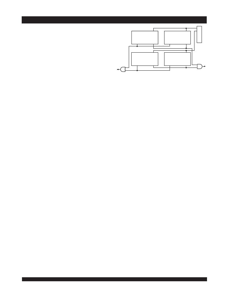
�MASTER� CE�
�Dual� Port�
�RAM�
�BUSY� (L)� BUSY� (R)�
�SLAVE� CE�
�Dual� Port�
�RAM�
�BUSY� (L)� BUSY� (R)�
�have� accessed� the� same� location� at� the� same� time.� It� also� allows� one� of� the�
�two� accesses� to� proceed� and� signals� the� other� side� that� the� RAM� is� “busy”.�
�The� BUSY� pin� can� then� be� used� to� stall� the� access� until� the� operation� on�
�BUSY� (L)�
�MASTER� CE�
�Dual� Port�
�RAM�
�BUSY� (L)� BUSY� (R)�
�SLAVE� CE�
�Dual� Port�
�RAM�
�BUSY� (L)� BUSY� (R)�
�BUSY� (R)�
�the� other� side� is� completed.� If� a� write� operation� has� been� attempted� from�
�the� side� that� receives� a� BUSY� indication,� the� write� signal� is� gated� internally�
�to� prevent� the� write� from� proceeding.�
�The� use� of� BUSY� logic� is� not� required� or� desirable� for� all� applications.�
�In� some� cases� it� may� be� useful� to� logically� OR� the� BUSY� outputs� together�
�and� use� any� BUSY� indication� as� an� interrupt� source� to� flag� the� event� of�
�an� illegal� or� illogical� operation.� If� the� write� inhibit� function� of� BUSY� logic� is�
�not� desirable,� the� BUSY� logic� can� be� disabled� by� placing� the� part� in� slave�
�mode� with� the� M/� S� pin.� Once� in� slave� mode� the� BUSY� pin� operates� solely�
�as� a� write� inhibit� input� pin.� Normal� operation� can� be� programmed� by� tying�
�the� BUSY� pins� HIGH.� If� desired,� unintended� write� operations� can� be�
�prevented� to� a� port� by� tying� the� BUSY� pin� for� that� port� LOW.�
�The� BUSY� outputs� on� the� IDT� 7024� SRAM� in� master� mode,� are� push-�
�pull� type� outputs� and� do� not� require� pull� up� resistors� to� operate.� If� these�
�RAMs� are� being� expanded� in� depth,� then� the� BUSY� indication� for� the�
�resulting� array� requires� the� use� of� an� external� AND� gate.�
�Width� Expansion� with� BUSY� Logic�
�Master/Slave� Arrays�
�When� expanding� an� IDT7024� RAM� array� in� width� while� using� BUSY�
�logic,� one� master� part� is� used� to� decide� which� side� of� the� RAM� array� will�
�receive� a� BUSY� indication,� and� to� output� that� indication.� Any� number� of�
�slaves� to� be� addressed� in� the� same� address� range� as� the� master,� use�
�the� BUSY� signal� as� a� write� inhibit� signal.� Thus� on� the� IDT7024� RAM� the�
�BUSY� pin� is� an� output� if� the� part� is� used� as� a� master� (M/� S� pin� =� V� IH� ),� and�
�the� BUSY� pin� is� an� input� if� the� part� used� as� a� slave� (M/� S� pin� =� V� IL� )� as� shown�
�in� Figure� 3.�
�If� two� or� more� master� parts� were� used� when� expanding� in� width,� a� split�
�decision� could� result� with� one� master� indicating� BUSY� on� one� side� of� the�
�array� and� another� master� indicating� BUSY� on� one� other� side� of� the� array.�
�This� would� inhibit� the� write� operations� from� one� port� for� part� of� a� word� and�
�inhibit� the� write� operations� from� the� other� port� for� the� other� part� of� the� word.�
�The� BUSY� arbitration,� on� a� master,� is� based� on� the� chip� enable� and�
�address� signals� only.� It� ignores� whether� an� access� is� a� read� or� write.� In�
�a� master/slave� array,� both� address� and� chip� enable� must� be� valid� long�
�enough� for� a� BUSY� flag� to� be� output� from� the� master� before� the� actual� write�
�pulse� can� be� initiated� with� either� the� R/� W� signal� or� the� byte� enables.� Failure�
�to� observe� this� timing� can� result� in� a� glitched� internal� write� inhibit� signal� and�
�corrupted� data� in� the� slave.�
�Semaphores�
�The� IDT7024� is� an� extremely� fast� Dual-Port� 4K� x� 16� CMOS� Static� RAM�
�with� an� additional� 8� address� locations� dedicated� to� binary� semaphore� flags.�
�These� flags� allow� either� processor� on� the� left� or� right� side� of� the� Dual-Port�
�RAM� to� claim� a� privilege� over� the� other� processor� for� functions� defined� by�
�the� system� designer’s� software.� As� an� example,� the� semaphore� can� be�
�2740� drw� 19�
�Figure� 3.� Busy� and� chip� enable� routing� for� both� width� and� depth�
�expansion� with� IDT7024� RAMs.�
�used� by� one� processor� to� inhibit� the� other� from� accessing� a� portion� of� the�
�Dual-Port� RAM� or� any� other� shared� resource.�
�The� Dual-Port� RAM� features� a� fast� access� time,� and� both� ports� are�
�completely� independent� of� each� other.� This� means� that� the� activity� on� the�
�left� port� in� no� way� slows� the� access� time� of� the� right� port.� Both� ports� are�
�identical� in� function� to� standard� CMOS� Static� RAM� and� can� be� read� from,�
�or� written� to,� at� the� same� time� with� the� only� possible� conflict� arising� from� the�
�simultaneous� writing� of,� or� a� simultaneous� READ/WRITE� of,� a� non-�
�semaphore� location.� Semaphores� are� protected� against� such� ambiguous�
�situations� and� may� be� used� by� the� system� program� to� avoid� any� conflicts�
�in� the� non-semaphore� portion� of� the� Dual-Port� RAM.� These� devices� have�
�an� automatic� power-down� feature� controlled� by� CE� ,� the� Dual-Port� RAM�
�enable,� and� SEM� ,� the� semaphore� enable.� The� CE� and� SEM� pins� control�
�on-chip� power� down� circuitry� that� permits� the� respective� port� to� go� into�
�standby� mode� when� not� selected.� This� is� the� condition� which� is� shown� in�
�Truth� Table� I� where� CE� and� SEM� =� V� IH� .�
�Systems� which� can� best� use� the� IDT7024� contain� multiple� processors�
�or� controllers� and� are� typically� very� high-speed� systems� which� are�
�software� controlled� or� software� intensive.� These� systems� can� benefit� from�
�a� performance� increase� offered� by� the� IDT7024's� hardware� semaphores,�
�which� provide� a� lockout� mechanism� without� requiring� complex� program-�
�ming.�
�Software� handshaking� between� processors� offers� the� maximum� in�
�system� flexibility� by� permitting� shared� resources� to� be� allocated� in� varying�
�configurations.� The� IDT7024� does� not� use� its� semaphore� flags� to� control�
�any� resources� through� hardware,� thus� allowing� the� system� designer� total�
�flexibility� in� system� architecture.�
�An� advantage� of� using� semaphores� rather� than� the� more� common�
�methods� of� hardware� arbitration� is� that� wait� states� are� never� incurred�
�in� either� processor.� This� can� prove� to� be� a� major� advantage� in� very�
�high-speed� systems.�
�How� the� Semaphore� Flags� Work�
�The� semaphore� logic� is� a� set� of� eight� latches� which� are� independent�
�of� the� Dual-Port� RAM.� These� latches� can� be� used� to� pass� a� flag,� or� token,�
�from� one� port� to� the� other� to� indicate� that� a� shared� resource� is� in� use.� The�
�semaphores� provide� a� hardware� assist� for� a� use� assignment� method�
�called� “Token� Passing� Allocation.”� In� this� method,� the� state� of� a� semaphore�
�latch� is� used� as� a� token� indicating� that� shared� resource� is� in� use.� If� the� left�
�processor� wants� to� use� this� resource,� it� requests� the� token� by� setting� the�
�latch.� This� processor� then� verifies� its� success� in� setting� the� latch� by� reading�
�18�
�6.42�
�相关PDF资料 |
PDF描述 |
|---|---|
| IDT7024S35G | IC SRAM 64KBIT 35NS 84PGA |
| IDT7024S25G | IC SRAM 64KBIT 25NS 84PGA |
| IDT7024S20G | IC SRAM 64KBIT 20NS 84PGA |
| IDT7024S17G | IC SRAM 64KBIT 17NS 84PGA |
| IDT7008L20JI | IC SRAM 512KBIT 20NS 84PLCC |
相关代理商/技术参数 |
参数描述 |
|---|---|
| IDT7024S55GB | 制造商:Integrated Device Technology Inc 功能描述:IC SRAM 64KBIT 55NS 84PGA |
| IDT7024S55J | 功能描述:IC SRAM 64KBIT 55NS 84PLCC RoHS:否 类别:集成电路 (IC) >> 存储器 系列:- 标准包装:72 系列:- 格式 - 存储器:RAM 存储器类型:SRAM - 同步 存储容量:9M(256K x 36) 速度:75ns 接口:并联 电源电压:3.135 V ~ 3.465 V 工作温度:-40°C ~ 85°C 封装/外壳:100-LQFP 供应商设备封装:100-TQFP(14x14) 包装:托盘 其它名称:71V67703S75PFGI |
| IDT7024S55J8 | 功能描述:IC SRAM 64KBIT 55NS 84PLCC RoHS:否 类别:集成电路 (IC) >> 存储器 系列:- 标准包装:72 系列:- 格式 - 存储器:RAM 存储器类型:SRAM - 同步 存储容量:9M(256K x 36) 速度:75ns 接口:并联 电源电压:3.135 V ~ 3.465 V 工作温度:-40°C ~ 85°C 封装/外壳:100-LQFP 供应商设备封装:100-TQFP(14x14) 包装:托盘 其它名称:71V67703S75PFGI |
| IDT7024S55JI | 功能描述:IC SRAM 64KBIT 55NS 84PLCC RoHS:否 类别:集成电路 (IC) >> 存储器 系列:- 标准包装:45 系列:- 格式 - 存储器:RAM 存储器类型:SRAM - 双端口,异步 存储容量:128K(8K x 16) 速度:15ns 接口:并联 电源电压:3 V ~ 3.6 V 工作温度:0°C ~ 70°C 封装/外壳:100-LQFP 供应商设备封装:100-TQFP(14x14) 包装:托盘 其它名称:70V25S15PF |
| IDT7024S55JI8 | 功能描述:IC SRAM 64KBIT 55NS 84PLCC RoHS:否 类别:集成电路 (IC) >> 存储器 系列:- 标准包装:72 系列:- 格式 - 存储器:RAM 存储器类型:SRAM - 同步 存储容量:9M(256K x 36) 速度:75ns 接口:并联 电源电压:3.135 V ~ 3.465 V 工作温度:-40°C ~ 85°C 封装/外壳:100-LQFP 供应商设备封装:100-TQFP(14x14) 包装:托盘 其它名称:71V67703S75PFGI |
发布紧急采购,3分钟左右您将得到回复。