- 您现在的位置:买卖IC网 > PDF目录4103 > IDT7133SA35J8 (IDT, Integrated Device Technology Inc)IC SRAM 32KBIT 35NS 68PLCC PDF资料下载
参数资料
| 型号: | IDT7133SA35J8 |
| 厂商: | IDT, Integrated Device Technology Inc |
| 文件页数: | 14/17页 |
| 文件大小: | 0K |
| 描述: | IC SRAM 32KBIT 35NS 68PLCC |
| 标准包装: | 250 |
| 格式 - 存储器: | RAM |
| 存储器类型: | SRAM - 双端口,异步 |
| 存储容量: | 32K(2K x 16) |
| 速度: | 35ns |
| 接口: | 并联 |
| 电源电压: | 4.5 V ~ 5.5 V |
| 工作温度: | 0°C ~ 70°C |
| 封装/外壳: | 68-LCC(J 形引线) |
| 供应商设备封装: | 68-PLCC(24x24) |
| 包装: | 带卷 (TR) |
| 其它名称: | 7133SA35J8 |
�� �
�
�IDT7133SA/LA,� IDT7143SA/LA�
�High-Speed� 2K� x� 16� Dual-Port� RAM�
�Military,� Industrial� and� Commercial� Temperature� Ranges�
�Functional� Description�
�The� IDT7133/43� provides� two� ports� with� separate� control,� address�
�and� I/O� pins� that� permit� independent� access� for� reads� or� writes� to� any�
�location� in� memory.� The� IDT7133/43� has� an� automatic� power� down�
�feature� controlled� by� CE� .� The� CE� controls� on-chip� power� down� circuitry�
�that� permits� the� respective� port� to� go� into� a� standby� mode� when� not�
�R/� W�
�BUSY�
�LEFT�
�R/� W�
�BUSY�
�IDT7133�
�MASTER�
�R/� W�
�BUSY�
�RIGHT�
�R/� W�
�BUSY�
�selected� (� CE� HIGH).� When� a� port� is� enabled,� access� to� the� entire�
�memory� array� is� permitted.� Non-contention� READ/WRITE� conditions�
�270� ?�
�V� CC�
�V� CC�
�270� ?�
�are� illustrated� in� Truth� Table� 1.�
�Busy� Logic�
�Busy� Logic� provides� a� hardware� indication� that� both� ports� of� the�
�RAM� have� accessed� the� same� location� at� the� same� time.� It� also� allows�
�R/� W�
�BUSY�
�IDT7143�
�SLAVE�
�R/� W�
�BUSY�
�2746� drw� 15�
�one� of� the� two� accesses� to� proceed� and� signals� the� other� side� that� the�
�RAM� is� “busy”.� The� BUSY� pin� can� then� be� used� to� stall� the� access� until�
�the� operation� on� the� other� side� is� completed.� If� a� write� operation� has�
�been� attempted� from� the� side� that� receives� a� BUSY� indication,� the�
�write� signal� is� gated� internally� to� prevent� the� write� from� proceeding.�
�The� use� of� BUSY� logic� is� not� required� or� desirable� for� all� applica-�
�tions.� In� some� cases� it� may� be� useful� to� logically� OR� the� BUSY� outputs�
�together� and� use� any� BUSY� indication� as� an� interrupt� source� to� flag� the�
�event� of� an� illegal� or� illogical� operation.� If� the� write� inhibit� function� of�
�BUSY� logic� is� not� desirable,� the� BUSY� logic� can� be� disabled� by� using�
�the� IDT7143� (SLAVE).� In� the� IDT7143,� the� BUSY� pin� operates� solely�
�as� a� write� inhibit� input� pin.� Normal� operation� can� be� programmed� by�
�tying� the� BUSY� pins� HIGH.� If� desired,� unintended� write� operations� can�
�be� prevented� to� a� port� by� tying� the� BUSY� pin� for� that� port� LOW.� The�
�BUSY� outputs� on� the� IDT� 7133� RAM� are� open� drain� and� require� pull-�
�up� resistors.�
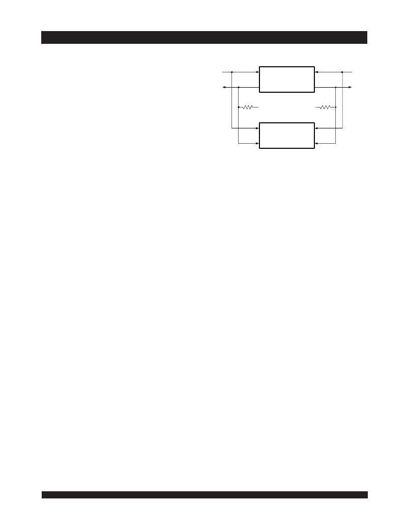
�Width� Expansion� with� Busy� Logic�
�Master/Slave� Arrays�
�When� expanding� an� IDT7133/43� RAM� array� in� width� while� using�
�BUSY� logic,� one� master� part� is� used� to� decide� which� side� of� the� RAM�
�array� will� receive� a� BUSY� indication,� and� to� output� that� indication.� Any�
�number� of� slaves� to� be� addressed� in� the� same� address� range� as� the�
�master,� use� the� BUSY� signal� as� a� write� inhibit� signal.� Thus� on� the�
�IDT7133� RAM� the� BUSY� pin� is� an� output� and� on� the� IDT7143� RAM,� the�
�BUSY� pin� is� an� input� (see� Figure� 3).�
�Figure� 4� .� Busy� and� chip� enable� routing� for� both� width� and� depth� expansion�
�with� the� IDT7133� (MASTER)� and� the� IDT7143� (SLAVE).�
�Expanding� the� data� bus� width� to� 32� bits� or� more� in� a� Dual-Port� RAM�
�system� implies� that� several� chips� will� be� active� at� the� same� time.� If� each�
�chip� includes� a� hardware� arbitrator,� and� the� addresses� for� each� chip�
�arrive� at� the� same� time,� it� is� possible� that� one� will� activate� its� BUSY� L�
�while� another� activates� its� BUSY� R� signal.� Both� sides� are� now� BUSY�
�and� the� CPUs� will� await� indefinitely� for� their� port� to� become� free.�
�To� avoid� the� “Busy� Lock-Out”� problem,� IDT� has� developed� a�
�MASTER/SLAVE� approach� where� only� one� hardware� arbitrator,� in� the�
�MASTER,� is� used.� The� SLAVE� has� BUSY� inputs� which� allow� an�
�interface� to� the� MASTER� with� no� external� components� and� with� a�
�speed� advantage� over� other� systems.�
�When� expanding� Dual-Port� RAMs� in� width,� the� writing� of� the� SLAVE�
�RAMs� must� be� delayed� until� after� the� BUSY� input� has� settled.�
�Otherwise,� the� SLAVE� chip� may� begin� a� write� cycle� during� a� contention�
�situation.� Conversely,� the� write� pulse� must� extend� a� hold� time� past�
�BUSY� to� ensure� that� a� write� cycle� takes� place� after� the� contention� is�
�resolved.� This� timing� is� inherent� in� all� Dual-Port� memory� systems� where�
�more� than� one� chip� is� active� at� the� same� time.�
�The� write� pulse� to� the� SLAVE� should� be� delayed� by� the� maximum�
�arbitration� time� of� the� MASTER.� If,� then,� a� contention� occurs,� the� write�
�to� the� SLAVE� will� be� inhibited� due� to� BUSY� from� the� MASTER.�
�14�
�6.42�
�相关PDF资料 |
PDF描述 |
|---|---|
| IDT7133LA45J8 | IC SRAM 32KBIT 45NS 68PLCC |
| IDT71V321L25JG | IC SRAM 16KBIT 25NS 52PLCC |
| IDT71V321L25J | IC SRAM 16KBIT 25NS 52PLCC |
| IDT71421LA25JI | IC SRAM 16KBIT 25NS 52PLCC |
| IDT7132LA25JI | IC SRAM 16KBIT 25NS 52PLCC |
相关代理商/技术参数 |
参数描述 |
|---|---|
| IDT7133SA35JG | 制造商:INTEGRATED DEVICE TECHNOLOGY 功能描述:SRAM DUAL PORT 2KX16 7133 PLCC68 制造商:INTEGRATED DEVICE TECHNOLOGY 功能描述:SRAM DUAL PORT 2KX16 7133 TUBE18 制造商:Integrated Device Technology Inc 功能描述:SRAM DUAL PORT 2KX16, 7133, PLCC68 制造商:INTEGRATED DEVICE TECHNOLOGY 功能描述:MEMORY, SRAM, 32KBIT, 35NS, PLCC-68; Memory Size:32Kbit; Memory Configuration:2K x 16; Supply Voltage Min:4.5V; Supply Voltage Max:5.5V; Memory Case Style:PLCC; No. of Pins:68; Access Time:35ns; Operating Temperature Min:0C ;RoHS Compliant: Yes |
| IDT7133SA35PF | 功能描述:IC SRAM 32KBIT 35NS 100TQFP RoHS:否 类别:集成电路 (IC) >> 存储器 系列:- 标准包装:72 系列:- 格式 - 存储器:RAM 存储器类型:SRAM - 同步 存储容量:9M(256K x 36) 速度:75ns 接口:并联 电源电压:3.135 V ~ 3.465 V 工作温度:-40°C ~ 85°C 封装/外壳:100-LQFP 供应商设备封装:100-TQFP(14x14) 包装:托盘 其它名称:71V67703S75PFGI |
| IDT7133SA35PF8 | 功能描述:IC SRAM 32KBIT 35NS 100TQFP RoHS:否 类别:集成电路 (IC) >> 存储器 系列:- 标准包装:72 系列:- 格式 - 存储器:RAM 存储器类型:SRAM - 同步 存储容量:9M(256K x 36) 速度:75ns 接口:并联 电源电压:3.135 V ~ 3.465 V 工作温度:-40°C ~ 85°C 封装/外壳:100-LQFP 供应商设备封装:100-TQFP(14x14) 包装:托盘 其它名称:71V67703S75PFGI |
| IDT7133SA35PFG | 功能描述:IC SRAM 32KBIT 35NS 100TQFP RoHS:是 类别:集成电路 (IC) >> 存储器 系列:- 标准包装:72 系列:- 格式 - 存储器:RAM 存储器类型:SRAM - 同步 存储容量:9M(256K x 36) 速度:75ns 接口:并联 电源电压:3.135 V ~ 3.465 V 工作温度:-40°C ~ 85°C 封装/外壳:100-LQFP 供应商设备封装:100-TQFP(14x14) 包装:托盘 其它名称:71V67703S75PFGI |
| IDT7133SA35PFG8 | 制造商:Integrated Device Technology Inc 功能描述:IC SRAM 32KBIT 35NS 100TQFP |
发布紧急采购,3分钟左右您将得到回复。