- 您现在的位置:买卖IC网 > PDF目录4116 > IDT71V321L35PF8 (IDT, Integrated Device Technology Inc)IC SRAM 16KBIT 35NS 64TQFP PDF资料下载
参数资料
| 型号: | IDT71V321L35PF8 |
| 厂商: | IDT, Integrated Device Technology Inc |
| 文件页数: | 13/15页 |
| 文件大小: | 0K |
| 描述: | IC SRAM 16KBIT 35NS 64TQFP |
| 标准包装: | 750 |
| 格式 - 存储器: | RAM |
| 存储器类型: | SRAM - 双端口,异步 |
| 存储容量: | 16K (2K x 8) |
| 速度: | 35ns |
| 接口: | 并联 |
| 电源电压: | 3 V ~ 3.6 V |
| 工作温度: | 0°C ~ 70°C |
| 封装/外壳: | 64-LQFP |
| 供应商设备封装: | 64-TQFP(14x14) |
| 包装: | 带卷 (TR) |
| 其它名称: | 71V321L35PF8 |
�� �
�
�IDT71V321/71V421S/L�
�High� Speed� 3.3V� 2K� x� 8� Dual-Port� Static� RAM� with� Interrupts�
�Functional� Description�
�The� IDT7V1321/IDT71V421� provides� two� ports� with� separate� control,�
�address� and� I/O� pins� that� permit� independent� access� for� reads� or� writes�
�to� any� location� in� memory.� The� IDT71V321/IDT71V421� has� an� automatic�
�power� down� feature� controlled� by� CE� .� The� CE� controls� on-chip� power�
�down� circuitry� that� permits� the� respective� port� to� go� into� a� standby� mode�
�when� not� selected� (� CE� =� V� IH� ).� When� a� port� is� enabled,� access� to� the� entire�
�memory� array� is� permitted.�
�Interrupts�
�If� the� user� chooses� the� interrupt� function,� a� memory� location� (mail� box�
�or� message� center)� is� assigned� to� each� port.� The� left� port� interrupt� flag�
�(� INT� L� )� is� asserted� when� the� right� port� writes� to� memory� location� 7FE�
�(HEX),� where� a� write� is� defined� as� the� CE� R� =� R/� W� R� =� V� IL� per� Truth� Table�
�Industrial� and� Commercial� Temperature� Ranges�
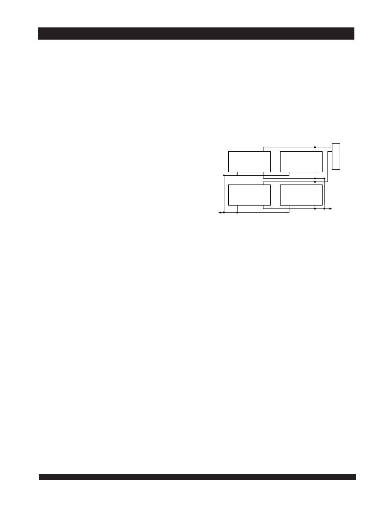
�being� expanded� in� depth,� then� the� BUSY� indication� for� the� resulting� array�
�requires� the� use� of� an� external� AND� gate.�
�Width� Expansion� with� Busy� Logic�
�Master/Slave� Arrays�
�When� expanding� an� SRAM� array� in� width� while� using� BUSY� logic,� one�
�master� part� is� used� to� decide� which� side� of� the� SRAM� array� will� receive�
�a� BUSY� indication.� Any� number� of� slaves� to� be� addressed� in� the� same�
�address� range� as� the� master,� use� the� BUSY� signal� as� a� write� inhibit� signal.�
�Thus� on� the� IDT71V321/IDT71V421� SRAMs� the� BUSY� pin� is� an� output�
�if� the� part� is� Master� (IDT71V321),� and� the� BUSY� pin� is� an� input� if� the� part�
�is� a� Slave� (IDT71V421)� as� shown� in� Figure� 3.�
�II.� The� left� port� clears� the� interrupt� by� accessing� address� location� 7FE� when�
�CE� L� =� OE� L� =� V� IL,� R/W� is� a� "don't� care".� Likewise,� the� right� port� interrupt�
�flag� (� INT� R� )� is� asserted� when� the� left� port� writes� to� memory� location� 7FF�
�MASTER�
�Dual� Port�
�RAM�
�BUSY� L�
�CE�
�BUSY� R�
�SLAVE�
�Dual� Port�
�RAM�
�BUSY� L�
�CE�
�BUSY� R�
�(HEX)� and� to� clear� the� interrupt� flag� (� INT� R� ),� the� right� port� must� access� the�
�memory� location� 7FF.� The� message� (8� bits)� at� 7FE� or� 7FF� is� user-defined,�
�since� it� is� an� addressable� SRAM� location.� If� the� interrupt� function� is� not� used,�
�address� locations� 7FE� and� 7FF� are� not� used� as� mail� boxes,� but� as� part�
�of� the� random� access� memory.� Refer� to� Truth� Table� II� for� the� interrupt�
�operation.�
�BUSY� L�
�MASTER�
�Dual� Port�
�RAM�
�BUSY� L�
�CE�
�BUSY� R�
�SLAVE�
�Dual� Port�
�RAM�
�BUSY� L�
�CE�
�BUSY� R�
�BUSY� R�
�3026� drw� 16�
�Busy� Logic�
�Busy� Logic� provides� a� hardware� indication� that� both� ports� of� the� RAM�
�have� accessed� the� same� location� at� the� same� time.� It� also� allows� one� of� the�
�two� accesses� to� proceed� and� signals� the� other� side� that� the� RAM� is� “Busy”.�
�The� BUSY� pin� can� then� be� used� to� stall� the� access� until� the� operation� on�
�the� other� side� is� completed.� If� a� write� operation� has� been� attempted� from�
�the� side� that� receives� a� busy� indication,� the� write� signal� is� gated� internally�
�to� prevent� the� write� from� proceeding.�
�The� use� of� BUSY� Logic� is� not� required� or� desirable� for� all� applications.�
�In� some� cases� it� may� be� useful� to� logically� OR� the� BUSY� outputs� together�
�and� use� any� BUSY� indication� as� an� interrupt� source� to� flag� the� event� of�
�an� illegal� or� illogical� operation.�
�The� BUSY� outputs� on� the� IDT71V321� RAM� master� are� totem-pole� type�
�outputs� and� do� not� require� pull-up� resistors� to� operate.� If� these� RAMs� are�
�Figure� 3.� Busy� and� chip� enable� routing� for� both� width� and� depth�
�expansion� with� IDT71V321� (Master)� and� (Slave)� IDT71V421� RAMs.�
�If� two� or� more� master� parts� were� used� when� expanding� in� width,� a� split�
�decision� could� result� with� one� master� indicating� BUSY� on� one� side� of� the�
�array� and� another� master� indicating� BUSY� on� one� other� side� of� the� array.�
�This� would� inhibit� the� write� operations� from� one� port� for� part� of� a� word� and�
�inhibit� the� write� operations� from� the� other� port� for� the� other� part� of� the� word.�
�The� BUSY� arbitration,� on� a� Master,� is� based� on� the� chip� enable� and�
�address� signals� only.� It� ignores� whether� an� access� is� a� read� or� write.� In�
�a� master/slave� array,� both� address� and� chip� enable� must� be� valid� long�
�enough� for� a� BUSY� flag� to� be� output� from� the� master� before� the� actual� write�
�pulse� can� be� initiated� with� either� the� R/� W� signal� or� the� byte� enables.� Failure�
�to� observe� this� timing� can� result� in� a� glitched� internal� write� inhibit� signal� and�
�corrupted� data� in� the� slave.�
�13�
�6.42�
�相关PDF资料 |
PDF描述 |
|---|---|
| 84952-9 | CONN FPC 9POS 1MM RT ANG SMD |
| IDT7133LA55J8 | IC SRAM 32KBIT 55NS 68PLCC |
| IDT70125L35J8 | IC SRAM 18KBIT 35NS 52PLCC |
| IDT70121L35J8 | IC SRAM 18KBIT 35NS 52PLCC |
| IDT7140SA20PF | IC SRAM 8KBIT 20NS 64TQFP |
相关代理商/技术参数 |
参数描述 |
|---|---|
| IDT71V321L35PFGI | 制造商:Integrated Device Technology Inc 功能描述:IC SRAM 16KBIT 35NS 64TQFP |
| IDT71V321L35PFGI8 | 制造商:Integrated Device Technology Inc 功能描述:IC SRAM 16KBIT 35NS 64TQFP |
| IDT71V321L35TF | 功能描述:IC SRAM 16KBIT 35NS 64STQFP RoHS:否 类别:集成电路 (IC) >> 存储器 系列:- 标准包装:72 系列:- 格式 - 存储器:RAM 存储器类型:SRAM - 同步 存储容量:9M(256K x 36) 速度:75ns 接口:并联 电源电压:3.135 V ~ 3.465 V 工作温度:-40°C ~ 85°C 封装/外壳:100-LQFP 供应商设备封装:100-TQFP(14x14) 包装:托盘 其它名称:71V67703S75PFGI |
| IDT71V321L35TF8 | 功能描述:IC SRAM 16KBIT 35NS 64STQFP RoHS:否 类别:集成电路 (IC) >> 存储器 系列:- 标准包装:72 系列:- 格式 - 存储器:RAM 存储器类型:SRAM - 同步 存储容量:9M(256K x 36) 速度:75ns 接口:并联 电源电压:3.135 V ~ 3.465 V 工作温度:-40°C ~ 85°C 封装/外壳:100-LQFP 供应商设备封装:100-TQFP(14x14) 包装:托盘 其它名称:71V67703S75PFGI |
| IDT71V321L55J | 功能描述:IC SRAM 16KBIT 55NS 52PLCC RoHS:否 类别:集成电路 (IC) >> 存储器 系列:- 标准包装:2,000 系列:MoBL® 格式 - 存储器:RAM 存储器类型:SRAM - 异步 存储容量:16M(2M x 8,1M x 16) 速度:45ns 接口:并联 电源电压:2.2 V ~ 3.6 V 工作温度:-40°C ~ 85°C 封装/外壳:48-VFBGA 供应商设备封装:48-VFBGA(6x8) 包装:带卷 (TR) |
发布紧急采购,3分钟左右您将得到回复。