- 您现在的位置:买卖IC网 > PDF目录4186 > IDT71V3559S80PFG8 (IDT, Integrated Device Technology Inc)IC SRAM 4MBIT 80NS 100TQFP PDF资料下载
参数资料
| 型号: | IDT71V3559S80PFG8 |
| 厂商: | IDT, Integrated Device Technology Inc |
| 文件页数: | 2/28页 |
| 文件大小: | 0K |
| 描述: | IC SRAM 4MBIT 80NS 100TQFP |
| 标准包装: | 1,000 |
| 格式 - 存储器: | RAM |
| 存储器类型: | SRAM - 同步 ZBT |
| 存储容量: | 4.5M(256K x 18) |
| 速度: | 80ns |
| 接口: | 并联 |
| 电源电压: | 3.135 V ~ 3.465 V |
| 工作温度: | 0°C ~ 70°C |
| 封装/外壳: | 100-LQFP |
| 供应商设备封装: | 100-TQFP(14x14) |
| 包装: | 带卷 (TR) |
| 其它名称: | 71V3559S80PFG8 |
第1页当前第2页第3页第4页第5页第6页第7页第8页第9页第10页第11页第12页第13页第14页第15页第16页第17页第18页第19页第20页第21页第22页第23页第24页第25页第26页第27页第28页
�� �
�
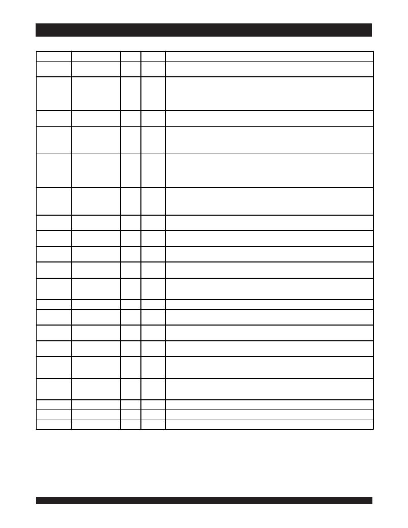
�IDT71V3557,� IDT71V3559,� 128K� x� 36,� 256K� x� 18,� 3.3V� Synchronous� SRAMs� with�
�ZBT?� Feature,� 3.3V� I/O,� Burst� Counter,� and� Flow-Through� Outputs� Commercial� and� Industrial� Temperature� Ranges�
�Pin� Definitions� (1)�
�Symbol�
�A� 0� -A� 17�
�ADV/� LD�
�Pin� Function�
�Address� Inputs�
�Advance� /� Load�
�I/O�
�I�
�I�
�Active�
�N/A�
�N/A�
�Description�
�Synchronous� Address� inputs.� The� address� register� is� triggered� by� a� combination� of� the� rising� edge� of� CLK,�
�ADV/� LD� low,� CEN� low,� and� true� chip� enables.�
�ADV/� LD� is� a� synchronous� input� that� is� used� to� load� the� internal� registers� with� new� address� and� control� when� it�
�is� sampled� low� at� the� rising� edge� of� clock� with� the� chip� selected.� When� ADV/� LD� is� low� with� the� chip�
�deselected,� any� burst� in� progress� is� terminated.� When� ADV/� LD� is� sampled� high� then� the� internal� burst�
�counter� is� advanced� for� any� burst� that� was� in� progress.� The� external� addresses� are� ignored� when� ADV/� LD� is�
�sampled� high.�
�R/� W�
�Read� /� Write�
�I�
�N/A�
�R/� W� signal� is� a� synchronous� input� that� identifies� whether� the� current� load� cycle� initiated� is� a� Read� or� Write�
�access� to� the� memory� array.� The� data� bus� activity� for� the� current� cycle� takes� place� one� clock� cycle� later.�
�CEN�
�Clock� Enable�
�I�
�LOW�
�Sy� nchronous� Clock� Enable� Input.� When� CEN� is� sampled� high,� all� other� synchronous� inputs,� including� clock�
�are� ignored� and� outputs� remain� unchanged.� The� effect� of� CEN� sampled� high� on� the� device� outputs� is� as� if�
�the� low� to� high� clock� transition� did� not� occur.� For� normal� operation,� CEN� must� be� samp� led� low� at� rising� edge�
�of� clock.�
�BW� 1� -� BW� 4�
�Individual� Byte�
�Write� Enables�
�I�
�LOW�
�Synchronous� byte� write� enables.� Each� 9-bit� byte� has� its� own� active� low� byte� write� enable.� On� load� write�
�cycles� (When� R/� W� and� ADV/� LD� are� sampled� low)� the� appropriate� byte� write� signal� (� BW� 1� -� BW� 4� )� must� be� valid.�
�The� byte� write� signal� must� also� be� valid� on� each� cycle� of� a� burst� write.� Byte� Write� signals� are� ignored� when�
�R/� W� is� sampled� high.� The� ap� propriate� byte(s)� of� data� are� written� into� the� device� one� cycle� later.� BW� 1� -� BW� 4�
�can� all� be� tied� low� if� always� doing� write� to� the� entire� 36-bit� word.�
�CE� 1� ,� CE� 2�
�Chip� Enables�
�I�
�LOW�
�Synchronous� active� low� chip� enable.� CE� 1� and� CE� 2� are� used� with� CE� 2� to� enable� the� IDT71V3557/59.� (� CE� 1� or�
�CE� 2� sampled� high� or� CE� 2� sampled� low)� and� ADV/� LD� low� at� the� rising� edge� of� clock,� initiates� a� deselect�
�cycle.� The� ZBT� TM� has� a� one� cycle� dese� lect,� i.e.,� the� data� bus� will� tri-state� one� clock� cycle� after� deselect� is�
�initiated.�
�CE� 2�
�CLK�
�Chip� Enable�
�Clock�
�I�
�I�
�HIGH�
�N/A�
�Synchronous� active� high� chip� enable.� CE� 2� is� used� with� CE� 1� and� CE� 2� to� enable� the� chip.� CE� 2� has� inverted�
�polarity� but� otherwise� identical� to� CE� 1� and� CE� 2� .�
�This� is� the� clock� input� to� the� IDT71V3557/59.� Except� for� OE� ,� all� timing� references� for� the� device� are� made�
�with� respect� to� the� rising� edge� of� CLK.�
�I/O� 0� -I/O� 31�
�Data� Input/Output�
�I/O�
�N/A�
�Data� input/output� (I/O)� pins.� The� data� input� path� is� registered,� triggered� by� the� rising� edge� of� CLK.� The� data�
�I/O� P1� -I/O� P4�
�output� path� is� flow-through� (no� output� register).�
�LBO�
�OE�
�TMS�
�TDI�
�TCK�
�TDO�
�TRST�
�Linear� Burst� Order�
�Output� Enable�
�Test� Mode� Select�
�Test� Data� Input�
�Test� Clock�
�Test� Data� Output�
�JTAG� Reset�
�(Optional)�
�I�
�I�
�I�
�I�
�I�
�O�
�I�
�LOW�
�LOW�
�N/A�
�N/A�
�N/A�
�N/A�
�LOW�
�Burst� order� selection� input.� When� LBO� is� high� the� Interleaved� burst� sequence� is� selected.� When� LBO� is� low�
�the� Linear� burst� sequence� is� selected.� LBO� is� a� static� input,� and� it� must� not� change� during� device� operation..�
�Asynchronous� output� enable.� OE� must� be� low� to� read� data� from� the� 71V3557/59.� When� OE� is� HIGH� the� I/O�
�pins� are� in� a� high-impedance� state.� OE� does� not� need� to� be� actively� controlled� for� read� and� write� cycles.� In�
�normal� operation,� OE� can� be� tied� low.�
�Gives� input� command� for� TAP� controller.� Sampled� on� rising� edge� of� TDK.� This� pin� has� an� internal� pullup.�
�Serial� input� of� registers� placed� between� TDI� and� TDO.� Sampled� on� rising� edge� of� TCK.� This� pin� has� an�
�internal� pullup.�
�Clock� input� of� TAP� controller.� Each� TAP� event� is� clocked.� Test� inputs� are� captured� on� rising� edge� of� TCK,�
�while� test� outputs� are� driven� from� the� falling� edge� of� TCK.� This� pin� has� an� internal� pullup.�
�Serial� output� of� registers� placed� between� TDI� and� TDO.� This� output� is� active� depending� on� the� state� of� the�
�TAP� controller.�
�Optional� Asynchronous� JTAG� reset.� Can� be� used� to� reset� the� TAP� controller,� but� not� required.� JTAG� reset�
�occurs� automatically� at� power� up� and� also� rese� ts� using� TMS� and� TCK� per� IEEE� 1149.1.� If� not� used� TRST� can�
�be� left� floating.� This� pin� has� an� internal� pullup.�
�Synchronous� sleep� mode� input.� ZZ� HIGH� will� gate� the� CLK� internally� and� power� down� the� IDT71V3557/3559� to�
�ZZ�
�Sleep� Mode�
�I�
�HIGH�
�its� lowest� power� consumption� level.� Data� retention� is� guaranteed� in� Sleep� Mode.� This� pin� has� an� internal�
�pulldown.�
�V� DD�
�V� DDQ�
�V� SS�
�Power� Supply�
�Power� Supply�
�Ground�
�N/A�
�N/A�
�N/A�
�N/A�
�N/A�
�N/A�
�3.3V� core� power� supply.�
�3.3V� I/O� Supply.�
�Ground.�
�5282� tbl� 02�
�NOTE:�
�1.� All� synchronous� inputs� must� meet� specified� setup� and� hold� times� with� respect� to� CLK.�
�6.42�
�相关PDF资料 |
PDF描述 |
|---|---|
| IDT71V35761S200PFG8 | IC SRAM 4MBIT 200MHZ 100TQFP |
| IDT71V35761S183PFG8 | IC SRAM 4MBIT 183MHZ 100TQFP |
| XC6VLX760-L1FFG1760I | IC FPGA VIRTEX 6 758K 1760FFGBGA |
| IDT71V35761S166PFG8 | IC SRAM 4MBIT 166MHZ 100TQFP |
| XC5VSX240T-1FFG1738I | IC FPGA VIRTEX 5 40K 1738FFGBGA |
相关代理商/技术参数 |
参数描述 |
|---|---|
| IDT71V3559S80PFGI | 功能描述:IC SRAM 4MBIT 80NS 100TQFP RoHS:是 类别:集成电路 (IC) >> 存储器 系列:- 标准包装:2,000 系列:MoBL® 格式 - 存储器:RAM 存储器类型:SRAM - 异步 存储容量:16M(2M x 8,1M x 16) 速度:45ns 接口:并联 电源电压:2.2 V ~ 3.6 V 工作温度:-40°C ~ 85°C 封装/外壳:48-VFBGA 供应商设备封装:48-VFBGA(6x8) 包装:带卷 (TR) |
| IDT71V3559S80PFGI8 | 功能描述:IC SRAM 4MBIT 80NS 100TQFP RoHS:是 类别:集成电路 (IC) >> 存储器 系列:- 标准包装:72 系列:- 格式 - 存储器:RAM 存储器类型:SRAM - 同步 存储容量:4.5M(256K x 18) 速度:133MHz 接口:并联 电源电压:3.135 V ~ 3.465 V 工作温度:0°C ~ 70°C 封装/外壳:100-LQFP 供应商设备封装:100-TQFP(14x20) 包装:托盘 |
| IDT71V3559S80PFI | 功能描述:IC SRAM 4MBIT 80NS 100TQFP RoHS:否 类别:集成电路 (IC) >> 存储器 系列:- 标准包装:576 系列:- 格式 - 存储器:闪存 存储器类型:闪存 - NAND 存储容量:512M(64M x 8) 速度:- 接口:并联 电源电压:2.7 V ~ 3.6 V 工作温度:-40°C ~ 85°C 封装/外壳:48-TFSOP(0.724",18.40mm 宽) 供应商设备封装:48-TSOP 包装:托盘 其它名称:497-5040 |
| IDT71V3559S80PFI8 | 功能描述:IC SRAM 4MBIT 80NS 100TQFP RoHS:否 类别:集成电路 (IC) >> 存储器 系列:- 标准包装:576 系列:- 格式 - 存储器:闪存 存储器类型:闪存 - NAND 存储容量:512M(64M x 8) 速度:- 接口:并联 电源电压:2.7 V ~ 3.6 V 工作温度:-40°C ~ 85°C 封装/外壳:48-TFSOP(0.724",18.40mm 宽) 供应商设备封装:48-TSOP 包装:托盘 其它名称:497-5040 |
| IDT71V3559S85BG | 功能描述:IC SRAM 4MBIT 85NS 119BGA RoHS:否 类别:集成电路 (IC) >> 存储器 系列:- 标准包装:2,000 系列:MoBL® 格式 - 存储器:RAM 存储器类型:SRAM - 异步 存储容量:16M(2M x 8,1M x 16) 速度:45ns 接口:并联 电源电压:2.2 V ~ 3.6 V 工作温度:-40°C ~ 85°C 封装/外壳:48-VFBGA 供应商设备封装:48-VFBGA(6x8) 包装:带卷 (TR) |
发布紧急采购,3分钟左右您将得到回复。