- 您现在的位置:买卖IC网 > PDF目录4106 > IDT71V67803S133BG8 (IDT, Integrated Device Technology Inc)IC SRAM 9MBIT 133MHZ 119BGA PDF资料下载
参数资料
| 型号: | IDT71V67803S133BG8 |
| 厂商: | IDT, Integrated Device Technology Inc |
| 文件页数: | 2/23页 |
| 文件大小: | 0K |
| 描述: | IC SRAM 9MBIT 133MHZ 119BGA |
| 标准包装: | 1,000 |
| 格式 - 存储器: | RAM |
| 存储器类型: | SRAM - 同步 |
| 存储容量: | 9M(512K x 18) |
| 速度: | 133MHz |
| 接口: | 并联 |
| 电源电压: | 3.135 V ~ 3.465 V |
| 工作温度: | 0°C ~ 70°C |
| 封装/外壳: | 119-BGA |
| 供应商设备封装: | 119-PBGA(14x22) |
| 包装: | 带卷 (TR) |
| 其它名称: | 71V67803S133BG8 |
�� �
�
�IDT71V67603,� IDT71V67803,� 256K� x� 36,� 512K� x� 18,� 3.3V� Synchronous� SRAMS� with�
�3.3V� I/O,� Pipelined� Outputs,� Single� Cycle� Deselect� Commercial� and� Industrial� Temperature� Ranges�
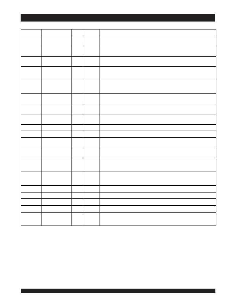
�Pin� Definitions� (1)�
�Symbol�
�A� 0� -A� 18�
�ADSC�
�Pin� Function�
�Address� Inputs�
�Address� Status�
�I/O�
�I�
�I�
�Active�
�N/A�
�LOW�
�Description�
�Synchronous� Address� inputs.� The� address� register� is� triggered� by� a� combination� of� the�
�rising� edge� of� CLK� and� ADSC� Low� or� ADSP� Low� and� CE� Low.�
�Synchronous� Address� Status� from� Cache� Controller.� ADSC� is� an� active� LOW� input� that� is�
�(Cache� Controller)�
�used� to� load� the� address� registers� with� new� addresses.�
�ADSP�
�ADV�
�Address� Status�
�(Processor)�
�Burst� Address�
�I�
�I�
�LOW�
�LOW�
�Synchronous� Address� Status� from� Processor.� ADSP� is� an� active� LOW� input� that� is� used� to�
�load� the� address� registers� with� new� addresses.� ADSP� is� gated� by� CE� .�
�Synchronous� Address� Advance.� ADV� is� an� active� LOW� input� that� is� used� to� advance� the�
�Advance�
�internal� burst� counter,� controlling� burst� access� after� the� initial� address� is� loaded.� When� the�
�input� is� HIGH� the� burst� counter� is� not� incremented;� that� is,� there� is� no� address� advance.�
�BWE�
�BW� 1� -� BW� 4�
�Byte� Write� Enable�
�Individual� Byte�
�I�
�I�
�LOW�
�LOW�
�Synchronous� byte� write� enable� gates� the� byte� write� inputs� BW� 1� -� BW� 4� .� If� BWE� is� LOW� at� the�
�rising� edge� of� CLK� then� BW� x� inputs� are� passed� to� the� next� stage� in� the� circuit.� If� BWE� is�
�HIGH� then� the� byte� write� inputs� are� blocked� and� only� GW� can� initiate� a� write� cycle.�
�Synchronous� byte� write� enables.� BW� 1� controls� I/O� 0-7� ,� I/O� P1� ,� BW� 2� controls� I/O� 8-15� ,� I/O� P2� ,� etc.�
�Write� Enables�
�Any� active� byte� write� causes� all� outputs� to� be� disabled.�
�CE�
�CLK�
�Chip� Enable�
�Clock�
�I�
�I�
�LOW�
�N/A�
�Synchronous� chip� enable.� CE� is� used� with� CS� 0� and� CS� 1� to� enable� the� IDT71V67603/7803.�
�CE� also� gates� ADSP� .�
�This� is� the� clock� input.� All� timing� references� for� the� device� are� made� with� respect� to� this�
�input.�
�CS� 0�
�CS� 1�
�GW�
�I/O� 0� -I/O� 31�
�Chip� Select� 0�
�Chip� Select� 1�
�Global� Write�
�Enable�
�Data� Input/Output�
�I�
�I�
�I�
�I/O�
�HIGH�
�LOW�
�LOW�
�N/A�
�Synchrono� us� active� HIGH� chip� select.� CS� 0� is� used� with� CE� and� CS� 1� to� enable� the� chip.�
�Synchronous� active� LOW� chip� select.� CS� 1� is� used� with� CE� and� CS� 0� to� enable� the� chip.�
�Synchronous� global� write� enable.� This� input� will� write� all� four� 9-bit� data� bytes� when� LOW�
�on� the� rising� edge� of� CLK.� GW� supersedes� individual� byte� write� enables.�
�Synchronous� data� input/output� (I/O)� pins.� Both� the� data� input� path� and� data� output� path� are�
�I/O� P1� -I/O� P4�
�registered� and� triggered� by� the� rising� edge� of� CLK.�
�LBO�
�Linear� Burst� Order�
�I�
�LOW�
�Asynchronous� burst� order� selection� input.� When� LBO� is� HIGH,� the� interleaved� burst�
�sequence� is� selected.� When� LBO� is� LOW� the� Line� ar� burst� sequence� is� selected.� LBO� is� a�
�static� input� and� must� not� change� state� while� the� device� is� operating.�
�OE�
�Output� Enable�
�I�
�LOW�
�Asynchronous� output� enable.� When� OE� is� LOW� the� data� output� drivers� are� enabled� on� the�
�I/O� pins� if� the� chip� is� also� selected.� When� OE� is� HIGH� the� I/O� pins� are� in� a� high-�
�impedance� state.�
�V� DD�
�V� DDQ�
�V� SS�
�NC�
�ZZ�
�Power� Supply�
�Power� Supply�
�Ground�
�No� Connect�
�Sleep� Mode�
�N/A�
�N/A�
�N/A�
�N/A�
�I�
�N/A�
�N/A�
�N/A�
�N/A�
�HIGH�
�3.3V� core� power� supply.�
�3.3V� I/O� Supply.�
�Ground.�
�NC� pins� are� not� electrically� connected� to� the� device.�
�Asynchronous� sleep� mode� input.� ZZ� HIGH� will� gate� the� CLK� internally� and� power� down� the�
�IDT71V67603/7803� to� its� lowest� power� consumption� level.� Data� retention� is� guaranteed� in�
�Sleep� Mode.�
�NOTE:�
�1.� All� synchronous� inputs� must� meet� specified� setup� and� hold� times� with� respect� to� CLK.�
�6.42�
�5310� tbl� 02�
�相关PDF资料 |
PDF描述 |
|---|---|
| MPC862PZQ100B | IC MPU POWERQUICC 100MHZ 357PBGA |
| IDT71V67703S85BG8 | IC SRAM 9MBIT 85NS 119BGA |
| MPC8349EVVALFB | IC MPU POWERQUICC II 672-TBGA |
| IDT71V67703S80BG8 | IC SRAM 9MBIT 80NS 119BGA |
| MPC8250ACZUMHBC | IC MPU POWERQUICC II 480-TBGA |
相关代理商/技术参数 |
参数描述 |
|---|---|
| IDT71V67803S133BGG | 功能描述:IC SRAM 9MBIT 133MHZ 119BGA RoHS:是 类别:集成电路 (IC) >> 存储器 系列:- 标准包装:72 系列:- 格式 - 存储器:RAM 存储器类型:SRAM - 同步 存储容量:9M(256K x 36) 速度:75ns 接口:并联 电源电压:3.135 V ~ 3.465 V 工作温度:-40°C ~ 85°C 封装/外壳:100-LQFP 供应商设备封装:100-TQFP(14x14) 包装:托盘 其它名称:71V67703S75PFGI |
| IDT71V67803S133BGG8 | 功能描述:IC SRAM 9MBIT 133MHZ 119BGA RoHS:是 类别:集成电路 (IC) >> 存储器 系列:- 标准包装:72 系列:- 格式 - 存储器:RAM 存储器类型:SRAM - 同步 存储容量:9M(256K x 36) 速度:75ns 接口:并联 电源电压:3.135 V ~ 3.465 V 工作温度:-40°C ~ 85°C 封装/外壳:100-LQFP 供应商设备封装:100-TQFP(14x14) 包装:托盘 其它名称:71V67703S75PFGI |
| IDT71V67803S133BQ | 功能描述:IC SRAM 9MBIT 133MHZ 165FBGA RoHS:否 类别:集成电路 (IC) >> 存储器 系列:- 标准包装:72 系列:- 格式 - 存储器:RAM 存储器类型:SRAM - 同步 存储容量:9M(256K x 36) 速度:75ns 接口:并联 电源电压:3.135 V ~ 3.465 V 工作温度:-40°C ~ 85°C 封装/外壳:100-LQFP 供应商设备封装:100-TQFP(14x14) 包装:托盘 其它名称:71V67703S75PFGI |
| IDT71V67803S133BQG | 功能描述:IC SRAM 9MBIT 133MHZ 165FBGA RoHS:是 类别:集成电路 (IC) >> 存储器 系列:- 标准包装:72 系列:- 格式 - 存储器:RAM 存储器类型:SRAM - 同步 存储容量:9M(256K x 36) 速度:75ns 接口:并联 电源电压:3.135 V ~ 3.465 V 工作温度:-40°C ~ 85°C 封装/外壳:100-LQFP 供应商设备封装:100-TQFP(14x14) 包装:托盘 其它名称:71V67703S75PFGI |
| IDT71V67803S133BQG8 | 功能描述:IC SRAM 9MBIT 133MHZ 165FBGA RoHS:是 类别:集成电路 (IC) >> 存储器 系列:- 标准包装:72 系列:- 格式 - 存储器:RAM 存储器类型:SRAM - 同步 存储容量:9M(256K x 36) 速度:75ns 接口:并联 电源电压:3.135 V ~ 3.465 V 工作温度:-40°C ~ 85°C 封装/外壳:100-LQFP 供应商设备封装:100-TQFP(14x14) 包装:托盘 其它名称:71V67703S75PFGI |
发布紧急采购,3分钟左右您将得到回复。