- 您现在的位置:买卖IC网 > PDF目录10039 > IDT723616L20PF8 (IDT, Integrated Device Technology Inc)IC FIFO TRPL BUS 64X36X2 128QFP PDF资料下载
参数资料
| 型号: | IDT723616L20PF8 |
| 厂商: | IDT, Integrated Device Technology Inc |
| 文件页数: | 2/26页 |
| 文件大小: | 0K |
| 描述: | IC FIFO TRPL BUS 64X36X2 128QFP |
| 标准包装: | 1,000 |
| 系列: | 7200 |
| 功能: | 同步 |
| 存储容量: | 4.6K(64 x 36 x2) |
| 数据速率: | 50MHz |
| 访问时间: | 20ns |
| 电源电压: | 4.5 V ~ 5.5 V |
| 工作温度: | 0°C ~ 70°C |
| 安装类型: | 表面贴装 |
| 封装/外壳: | 128-LQFP |
| 供应商设备封装: | 128-TQFP(14x20) |
| 包装: | 带卷 (TR) |
| 其它名称: | 723616L20PF8 |
10
COMMERCIALANDINDUSTRIAL
TEMPERATURERANGES
IDT723616 CMOS TRIPLE BUS SyncFIFO
WITH
BUS-MATCHING AND BYTE SWAPPING 64 x 36 x 2
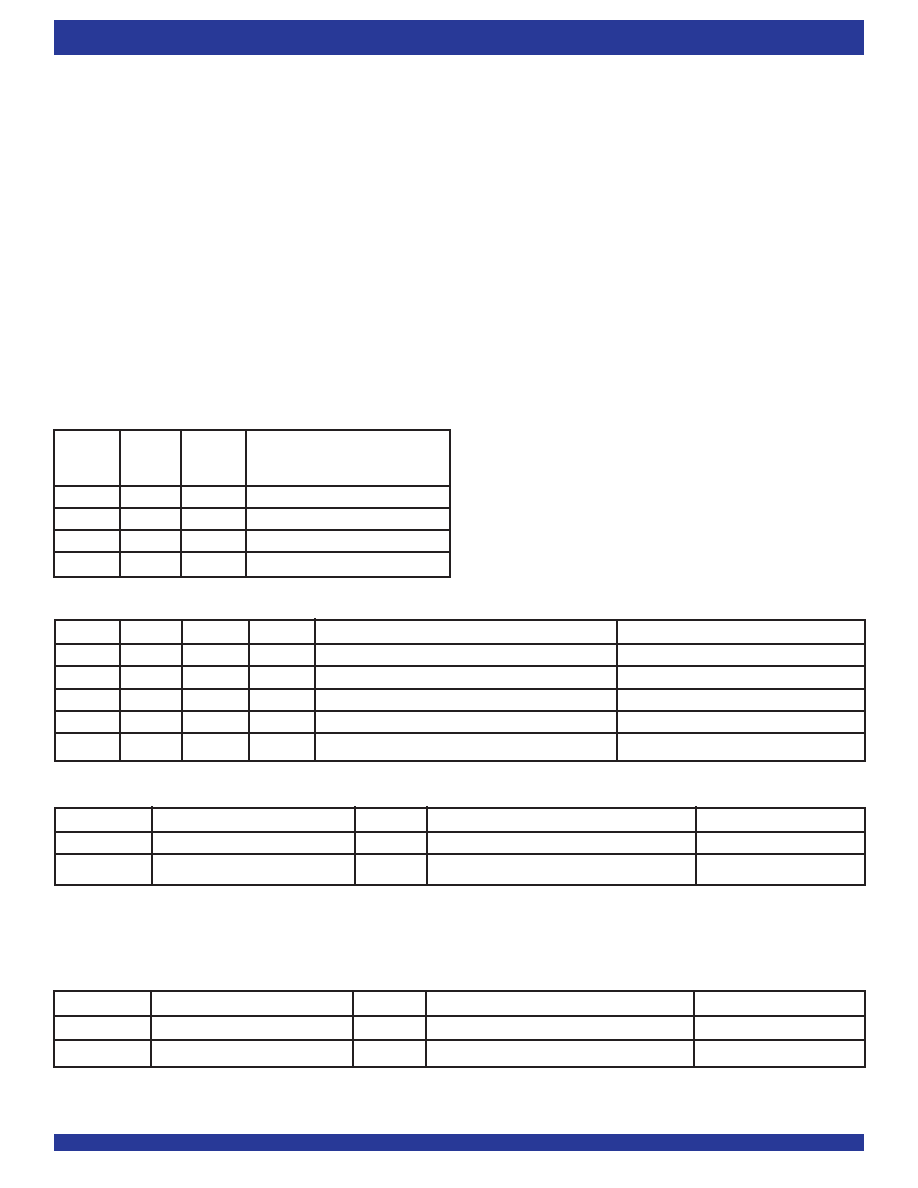
TABLE 4 — PORT-C ENABLE FUNCTION TABLE
NOTE:
1. At no time during the operation of the FIFO is it permissible to apply a LOW logic level simultaneously to both SIZ0 and SIZ1, nor is it permissible to apply a HIGH logic level
simultaneously to both these inputs. These state combinations are reserved.
WENC
SIZ1, SIZ0
CLKC
C0-C17 Inputs
Port Functions
L
X
In High-Impedance State
None
H
One or the other LOW(1)
↑
In High-Impedance State
FIFO2 write
SIGNALDESCRIPTIONS
RESET
The IDT723616 is reset by taking the reset (
RST) input LOW for at least
four Port A clock (CLKA), four Port B clock (CLKB) and four Port C clock
(CLKC) LOW-to-HIGH transitions. The reset input can switch asynchro-
nously to the clocks. A device reset initializes the internal read and write
pointers of each FIFO and forces the full flags (
FFA, FFC) LOW, the empty
flags (
EFA, EFB) LOW, the Almost-Empty flags (AEA, AEB) LOW and the
Almost-Full flags (
AFA, AFC) HIGH. After a reset, FFA is set HIGH after
two LOW-to-HIGH transitions of CLKA and FFC is set HIGH after two
LOW-to-HIGH transitions of CLKC. The device must be reset after power
up before data is written to its memory.
A LOW-to-HIGH transition on the
RST input loads the Almost-Full and
Almost-Empty Offset register (X) with the values selected by the flag-
select (FS0, FS1) inputs. The values that can be loaded into the registers
are shown in Table 1.
TABLE 2 — PORT-A ENABLE FUNCTION TABLE
FIFO WRITE/READ OPERATION
The state of Port A data A0-A35 outputs is controlled by the Port A chip
select (
CSA)andthePortAwrite/readselect(W/RA).TheA0-A35outputsare
in the high-impedance state when either
CSA or W/RA is HIGH. The A0-A35
outputs are active when both CSA and W/
RA are LOW. Data is loaded into
FIFO1 from the A0-A35 inputs on a LOW-to-HIGH transition of CLKA when
CSA is LOW, W/RA is HIGH, ENA is HIGH, and FFA is HIGH. Data is read
fromFIFO2totheA0-A35outputsbyaLOW-to-HIGHtransitionofCLKAwhen
CSA is LOW, W/
RA is LOW, ENA is HIGH, and EFA is HIGH (see Table 2).
The state of the Port B data (B0-B17) outputs is controlled by Port B read
select (RENB). The B0-B17 outputs are in the high-impedance state when
REN is LOW. The B0-B17 outputs are active when REN IS HIGH. Data is
read from FIFO1 to the B0-B17 outputs by a LOW-to-HIGH transition of
CLKB when RENB is HIGH,
EFB is HIGH, and either SIZ0 or SIZ1 is LOW
(see Table 3).
Data is loaded into FIFO2 from the C0-C17 inputs on a LOW-to-HIGH
transition of CLKC when WENC is HIGH,
FFC is HIGH, and either SIZ0 or
SIZ1 is LOW (see Table 4).
ThesetupandholdtimeconstraintstothePortClocksforthePortAchipselect
(CSA) and write/read selects (W/
RA, RENB, WENC) are only for enabling
write and read operations and are not related to high-impedance control of the
data outputs. If a port enable is LOW during a clock cycle, the Port Chip select
(for Port A) and write/read select (for all ports) can change states during the
setup and hold time window of the cycle.
TABLE 1 — FLAG PROGRAMMING
TABLE 3 — PORT-B ENABLE FUNCTION TABLE
NOTE:
1. At no time during the operation of the FIFO is it permissible to apply a LOW logic level simultaneously to both SIZ0 and SIZ1, nor is it permissible to apply a HIGH logic level
simultaneously to both these inputs. These state combinations are reserved.
ALMOST-FULL AND
FS1
FS0
RST
ALMOST-EMPTY FLAG
OFFSET REGISTER (X)
HH
↑
16
HL
↑
12
LH
↑
8
LL
↑
4
CSA
W/
RA
ENA
CLKA
A0-A35 Outputs
Port Functions
H
X
In High-Impedance State
None
L
H
L
X
In High-Impedance State
None
LH
H
↑
In High-Impedance State
FIFO1 Write
L
X
Active, FIFO2 Output Register
None
LL
H
↑
Active, FIFO2 Output Register
FIFO2 Read
RENB
SIZ1, SIZ0
CLKB
B0-B17 Outputs
Port Functions
L
X
In High-Impedance State
None
H
One or the other LOW(1)
↑
Active, FIFO1 Output Register
FIFO1 read
相关PDF资料 |
PDF描述 |
|---|---|
| MS27497P18F35P | CONN RCPT 66POS WALL MNT W/PINS |
| MS27472T14A18P | CONN RCPT 18POS WALL MT W/PINS |
| IDT72841L25TFI8 | IC FIFO SYNC 4KX9 25NS 64QFP |
| MS27466T13A8P | CONN RCPT 8POS WALL MT W/PINS |
| MS27484T14B35SD | CONN PLUG 37POS STRAIGHT W/SCKT |
相关代理商/技术参数 |
参数描述 |
|---|---|
| IDT723616L20PFI | 功能描述:IC FIFO TRPL BUS 64X36X2 128QFP RoHS:否 类别:集成电路 (IC) >> 逻辑 - FIFO 系列:7200 标准包装:90 系列:7200 功能:同步 存储容量:288K(16K x 18) 数据速率:100MHz 访问时间:10ns 电源电压:4.5 V ~ 5.5 V 工作温度:0°C ~ 70°C 安装类型:表面贴装 封装/外壳:64-LQFP 供应商设备封装:64-TQFP(14x14) 包装:托盘 其它名称:72271LA10PF |
| IDT723616L20PFI8 | 功能描述:IC FIFO TRPL BUS 64X36X2 128QFP RoHS:否 类别:集成电路 (IC) >> 逻辑 - FIFO 系列:7200 标准包装:90 系列:7200 功能:同步 存储容量:288K(16K x 18) 数据速率:100MHz 访问时间:10ns 电源电压:4.5 V ~ 5.5 V 工作温度:0°C ~ 70°C 安装类型:表面贴装 封装/外壳:64-LQFP 供应商设备封装:64-TQFP(14x14) 包装:托盘 其它名称:72271LA10PF |
| IDT723622L12PF | 功能描述:IC FIFO SYNC 256X36X2 120QFP RoHS:否 类别:集成电路 (IC) >> 逻辑 - FIFO 系列:7200 标准包装:90 系列:7200 功能:同步 存储容量:288K(16K x 18) 数据速率:100MHz 访问时间:10ns 电源电压:4.5 V ~ 5.5 V 工作温度:0°C ~ 70°C 安装类型:表面贴装 封装/外壳:64-LQFP 供应商设备封装:64-TQFP(14x14) 包装:托盘 其它名称:72271LA10PF |
| IDT723622L12PF8 | 功能描述:IC FIFO SYNC 256X36X2 120QFP RoHS:否 类别:集成电路 (IC) >> 逻辑 - FIFO 系列:7200 标准包装:90 系列:7200 功能:同步 存储容量:288K(16K x 18) 数据速率:100MHz 访问时间:10ns 电源电压:4.5 V ~ 5.5 V 工作温度:0°C ~ 70°C 安装类型:表面贴装 封装/外壳:64-LQFP 供应商设备封装:64-TQFP(14x14) 包装:托盘 其它名称:72271LA10PF |
| IDT723622L12PQF | 功能描述:IC FIFO SYNC 256X36X2 132QFP RoHS:否 类别:集成电路 (IC) >> 逻辑 - FIFO 系列:7200 标准包装:90 系列:7200 功能:同步 存储容量:288K(16K x 18) 数据速率:100MHz 访问时间:10ns 电源电压:4.5 V ~ 5.5 V 工作温度:0°C ~ 70°C 安装类型:表面贴装 封装/外壳:64-LQFP 供应商设备封装:64-TQFP(14x14) 包装:托盘 其它名称:72271LA10PF |
发布紧急采购,3分钟左右您将得到回复。