- 您现在的位置:买卖IC网 > PDF目录9986 > IDT72825LB15PFI (IDT, Integrated Device Technology Inc)IC FIFO SYNC DL 1024X18 128TQFP PDF资料下载
参数资料
| 型号: | IDT72825LB15PFI |
| 厂商: | IDT, Integrated Device Technology Inc |
| 文件页数: | 25/26页 |
| 文件大小: | 0K |
| 描述: | IC FIFO SYNC DL 1024X18 128TQFP |
| 标准包装: | 72 |
| 系列: | 7200 |
| 功能: | 同步 |
| 存储容量: | 18.4K(1K x 18) |
| 数据速率: | 67MHz |
| 访问时间: | 15ns |
| 电源电压: | 4.5 V ~ 5.5 V |
| 工作温度: | -40°C ~ 85°C |
| 安装类型: | 表面贴装 |
| 封装/外壳: | 128-LQFP |
| 供应商设备封装: | 128-TQFP(14x20) |
| 包装: | 托盘 |
| 其它名称: | 72825LB15PFI |
COMMERCIALANDINDUSTRIAL
TEMPERATURERANGES
IDT72805LB/72815LB/72825LB/72835LB/72845LB CMOS Dual SyncFIFOTM
256 x 18, 512 x 18, 1,024 x 18, 2,048 x 18 and 4,096 x 18
8
JANUARY 13, 2009
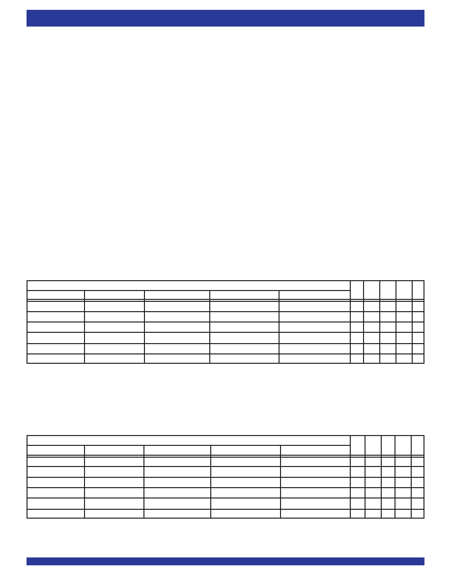
TABLE 1 — STATUS FLAGS FOR IDT STANDARD MODE
Number of Words in FIFO
IDT72805LB
IDT72815LB
IDT72825LB
IDT72835LB
IDT72845LB
FF PAF HF PAE EF
00
0
H
L
1 to n(1)
HH
H
L
H
(n + 1) to 128
(n + 1) to 256
(n + 1) to 512
(n + 1) to 1,024
(n + 1) to 2,048
H
129 to (256-(m+1))(2)
257 to (512-(m+1))(2)
513 to (1,024-(m+1))(2)
1,025 to (2,048-(m+1))(2)
2,049 to (4,096-(m+1))(2)
HH
L
H
(256-m) to 255
(512-m) to 511
(1,024-m) to 1,023
(2,048-m) to 2,047
(4,096-m) to 4,095
H
L
H
256
512
1,024
2,048
4,096
L
H
TABLE 2 — STATUS FLAGS FOR FWFT MODE
Number of Words in FIFO
IDT72805LB
IDT72815LB
IDT72825LB
IDT72835LB
IDT72845LB
IR PAF HF PAE OR
00
0
L
H
L
H
1 to (n + 1)(1)
LH
HL
L
(n + 2) to 129
(n + 2) to 257
(n + 2) to 513
(n + 2) to 1,025
(n + 2) to 2,049
L
H
L
130 to (257-(m+1))(2)
258 to (513-(m+1))(2)
514 to (1,025-(m+1))(2)
1,026 to (2,049-(m+1))(2)
2,050 to (4,097-(m+1))(2)
LHLHL
(257-m) to 256
(513-m) to 512
(1,025-m) to 1,024
(2,049-m) to 2,048
(4,097-m) to 4,096
LL
L
H
L
257
513
1,025
2,049
4,097
H
L
H
L
NOTES:
1. n = Empty offset (Default Values : IDT72805LB n = 31, IDT72815LB n = 63, IDT72825LB/72835LB/72845LB n = 127)
2. m = Full Offset (Default Values : IDT72805LB m = 31, IDT72815LB m = 63, IDT72825LB/72835LB/72845LB m = 127)
NOTES:
1. n = Empty offset (Default Values : IDT72805LB n=31, IDT72815LB n = 63, IDT72825LB/72835LB/72845LB n = 127)
2. m = Full offset (Default Values : IDT72805LB m=31, IDT72815LB m = 63, IDT72825LB/72835LB/72845LB m = 127)
by bringing the
LD pin HIGH, the FIFO is returned to normal read/write
operation. When the
LD pin and WEN are again set LOW, the next offset
register in sequence is written.
The contents of the offset registers can be read on the data output lines
Q0-Q11 when the
LD pin is set LOW and REN is set LOW. Data can then be
read on the next LOW-to-HIGH transition of RCLK. The first transition of
RCLK will present the Empty Offset value to the data output lines. The next
transition of RCLK will present the Full offset value. Offset register content
can be read out in the IDT Standard mode only. It cannot be read in the
FWFT mode.
SYNCHRONOUS vs ASYNCHRONOUS PROGRAMMABLE FLAG TIM-
ING SELECTION
The IDT72805LB/72815LB/72825LB/72835LB/72845LB can be config-
ured during the "Configuration at Reset" cycle described in Table 3 with
either asynchronous or synchronous timing for
PAE and PAF flags.
If asynchronous
PAE/PAF configuration is selected (as per Table 3), the
PAE is asserted LOW on the LOW-to-HIGH transition of RCLK. PAE is reset
to HIGH on the LOW-to-HIGH transition of WCLK. Similarly, the
PAF is
asserted LOW on the LOW-to-HIGH transition of WCLK and
PAF is reset
to HIGH on the LOW-to-HIGH transition of RCLK. For detail timing dia-
grams, see Figure 13 for asynchronous
PAE timing and Figure 14 for
asynchronous
PAF timing.
If synchronous
PAE/PAF configuration is selected, the PAE is asserted
and updated on the rising edge of RCLK only and not WCLK. Similarly,
PAF
is asserted and updated on the rising edge of WCLK only and not RCLK. For
detail timing diagrams, see Figure 22 for synchronous
PAE timing and
Figure 23 for synchronous
PAF timing.
REGISTER-BUFFERED FLAG OUTPUT SELECTION
The IDT72805LB/72815LB/72825LB/72835LB/72845LB can be config-
ured during the "Configuration at Reset" cycle described in Table 4 with
single, double or triple register-buffered flag output signals. The various
combinations available are described in Table 4 and Table 5. In general,
going from single to double or triple buffered flag outputs removes the
possibility of metastable flag indications on boundary states (i.e, empty or
full conditions). The trade-off is the addition of clock cycle delays for the
respective flag to be asserted. Not all combinations of register-buffered flag
outputs are supported. Register-buffered outputs apply to the Empty Flag
and Full Flag only. Partial flags are not effected. Table 4 and Table 5
summarize the options available.
相关PDF资料 |
PDF描述 |
|---|---|
| MS27474E16F55P | CONN RCPT 55POS JAM NUT W/PINS |
| IDT72825LB10PF | IC FIFO SYNC DL 1024X18 128TQFP |
| VE-26H-IW-F2 | CONVERTER MOD DC/DC 52V 100W |
| MS27466T9A98P | CONN RCPT 3POS WALL MT W/PINS |
| IDT72V831L15PFI | IC SYNC FIFO 2048X9 15NS 64QFP |
相关代理商/技术参数 |
参数描述 |
|---|---|
| IDT72825LB15PFI8 | 功能描述:IC FIFO SYNC DL 1024X18 128TQFP RoHS:否 类别:集成电路 (IC) >> 逻辑 - FIFO 系列:7200 标准包装:90 系列:7200 功能:同步 存储容量:288K(16K x 18) 数据速率:100MHz 访问时间:10ns 电源电压:4.5 V ~ 5.5 V 工作温度:0°C ~ 70°C 安装类型:表面贴装 封装/外壳:64-LQFP 供应商设备封装:64-TQFP(14x14) 包装:托盘 其它名称:72271LA10PF |
| IDT72825LB25BG | 功能描述:IC FIFO SYNC DL 1024X18 121BGA RoHS:否 类别:集成电路 (IC) >> 逻辑 - FIFO 系列:7200 标准包装:15 系列:74F 功能:异步 存储容量:256(64 x 4) 数据速率:- 访问时间:- 电源电压:4.5 V ~ 5.5 V 工作温度:0°C ~ 70°C 安装类型:通孔 封装/外壳:24-DIP(0.300",7.62mm) 供应商设备封装:24-PDIP 包装:管件 其它名称:74F433 |
| IDT72825LB25BG8 | 功能描述:IC FIFO SYNC DL 1024X18 121BGA RoHS:否 类别:集成电路 (IC) >> 逻辑 - FIFO 系列:7200 标准包装:15 系列:74F 功能:异步 存储容量:256(64 x 4) 数据速率:- 访问时间:- 电源电压:4.5 V ~ 5.5 V 工作温度:0°C ~ 70°C 安装类型:通孔 封装/外壳:24-DIP(0.300",7.62mm) 供应商设备封装:24-PDIP 包装:管件 其它名称:74F433 |
| IDT72825LB25PF | 功能描述:IC FIFO SYNC DL 1024X18 128TQFP RoHS:否 类别:集成电路 (IC) >> 逻辑 - FIFO 系列:7200 标准包装:90 系列:7200 功能:同步 存储容量:288K(16K x 18) 数据速率:100MHz 访问时间:10ns 电源电压:4.5 V ~ 5.5 V 工作温度:0°C ~ 70°C 安装类型:表面贴装 封装/外壳:64-LQFP 供应商设备封装:64-TQFP(14x14) 包装:托盘 其它名称:72271LA10PF |
| IDT72825LB25PF8 | 功能描述:IC FIFO SYNC DL 1024X18 128TQFP RoHS:否 类别:集成电路 (IC) >> 逻辑 - FIFO 系列:7200 标准包装:90 系列:7200 功能:同步 存储容量:288K(16K x 18) 数据速率:100MHz 访问时间:10ns 电源电压:4.5 V ~ 5.5 V 工作温度:0°C ~ 70°C 安装类型:表面贴装 封装/外壳:64-LQFP 供应商设备封装:64-TQFP(14x14) 包装:托盘 其它名称:72271LA10PF |
发布紧急采购,3分钟左右您将得到回复。