- 您现在的位置:买卖IC网 > PDF目录9896 > IDT72V2113L6PF8 (IDT, Integrated Device Technology Inc)IC FIFO SUPERSYNCII 6NS 80-TQFP PDF资料下载
参数资料
| 型号: | IDT72V2113L6PF8 |
| 厂商: | IDT, Integrated Device Technology Inc |
| 文件页数: | 35/46页 |
| 文件大小: | 0K |
| 描述: | IC FIFO SUPERSYNCII 6NS 80-TQFP |
| 标准包装: | 750 |
| 系列: | 72V |
| 功能: | 同步 |
| 存储容量: | 4.7Mb(262k x 18) |
| 访问时间: | 4ns |
| 电源电压: | 3.15 V ~ 3.45 V |
| 工作温度: | 0°C ~ 70°C |
| 安装类型: | 表面贴装 |
| 封装/外壳: | 80-LQFP |
| 供应商设备封装: | 80-TQFP(14x14) |
| 包装: | 带卷 (TR) |
| 其它名称: | 72V2113L6PF8 |
第1页第2页第3页第4页第5页第6页第7页第8页第9页第10页第11页第12页第13页第14页第15页第16页第17页第18页第19页第20页第21页第22页第23页第24页第25页第26页第27页第28页第29页第30页第31页第32页第33页第34页当前第35页第36页第37页第38页第39页第40页第41页第42页第43页第44页第45页第46页
40
IDT72V263/273/283/293/103/113 3.3V HIGH DENSITY SUPERSYNC IITM NARROW BUS FIFO
8K x 18, 16K x 9/18, 32K x 9/18, 64K x 9/18, 128K x 9/18, 256K x 9/18, 512K x9
COMMERCIAL AND INDUSTRIAL
TEMPERATURE RANGES
IDT72V2103/72V2113 3.3V HIGH DENSITY SUPERSYNC IITM NARROW BUS FIFO
131,072 x 18/262,144 x 9, 262,144 x 18/524,288 x 9
JUNE 1, 2010
DEPTH EXPANSION CONFIGURATION (FWFT MODE ONLY)
The IDT72V2103 can easily be adapted to applications requiring depths
greater than 131,072 when the x18 Input or x18 Output bus Width is selected
and262,144fortheIDT72V2113.Whenbothx9Inputandx9OutputbusWidths
areselected,depthsgreaterthan262,144canbeadaptedfortheIDT72V2103
and524,288fortheIDT72V2113.InFWFTmode,theFIFOscanbeconnected
in series (the data outputs of one FIFO connected to the data inputs of the next)
with no external logic necessary. The resulting configuration provides a total
depth equivalent to the sum of the depths associated with each single FIFO.
Figure30showsadepthexpansionusingtwoIDT72V2103/72V2113devices.
CareshouldbetakentoselectFWFTmodeduringMasterResetforallFIFOs
in the depth expansion configuration. The first word written to an empty
configuration will pass from one FIFO to the next ("ripple down") until it finally
appears at the outputs of the last FIFO in the chain–no read operation is
necessarybuttheRCLKofeachFIFOmustbefree-running.Eachtimethedata
word appears at the outputs of one FIFO, that device's
OR line goes LOW,
enabling a write to the next FIFO in line.
For an empty expansion configuration, the amount of time it takes for
ORof
the last FIFO in the chain to go LOW (i.e. valid data to appear on the last FIFO's
outputs) after a word has been written to the first FIFO is the sum of the delays
for each individual FIFO:
(N – 1)*(4*transfer clock) + 3*TRCLK
whereNisthenumberofFIFOsintheexpansionandTRCLKistheRCLKperiod.
Note that extra cycles should be added for the possibility that the tSKEW1
specificationisnotmetbetweenWCLKandtransferclock,orRCLKandtransfer
clock, for the
OR flag.
The "ripple down" delay is only noticeable for the first word written to an
empty depth expansion configuration. There will be no delay evident for
subsequent words written to the configuration.
The first free location created by reading from a full depth expansion
configuration will "bubble up" from the last FIFO to the previous one until it
finally moves into the first FIFO of the chain. Each time a free location is
created in one FIFO of the chain, that FIFO's
IR line goes LOW, enabling the
preceding FIFO to write a word to fill it.
Forafullexpansionconfiguration,theamountoftimeittakesfor
IRofthefirst
FIFO in the chain to go LOW after a word has been read from the last FIFO is
the sum of the delays for each individual FIFO:
(N – 1)*(3*transfer clock) + 2 TWCLK
where N is the number of FIFOs in the expansion and TWCLK is the WCLK
period.NotethatextracyclesshouldbeaddedforthepossibilitythatthetSKEW1
specificationisnotmetbetweenRCLKandtransferclock,orWCLKandtransfer
clock, for the
IR flag.
The Transfer Clock line should be tied to either WCLK or RCLK, whichever
is faster. Both these actions result in data moving, as quickly as possible, to the
end of the chain and free locations to the beginning of the chain.
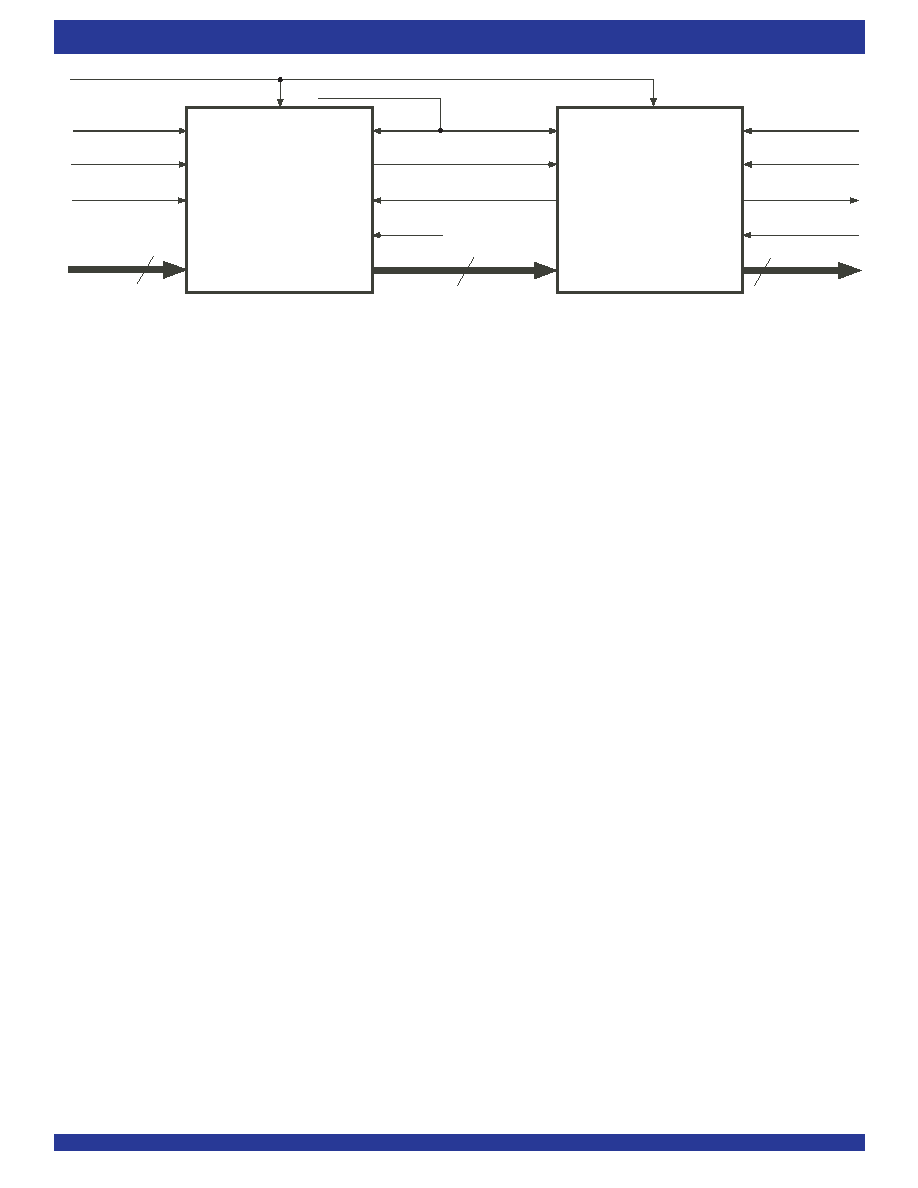
Figure 30. Block Diagram of Depth Expansion
For the x18 Input or x18 Output bus Width: 262,144 x 18 and 524,288 x 18
For both x9 Input and x9 Output bus Widths: 524,288 x 9 and 1,048,576 x 9
Dn
INPUT READY
WRITE ENABLE
WRITE CLOCK
WEN
WCLK
IR
DATA IN
RCLK
READ CLOCK
RCLK
REN
OE
OUTPUT ENABLE
OUTPUT READY
Qn
Dn
IR
GND
WEN
WCLK
OR
REN
OE
Qn
READ ENABLE
OR
DATA OUT
IDT
72V2103
72V2113
TRANSFER CLOCK
6119 drw33
n
FWFT/SI
IDT
72V2103
72V2113
相关PDF资料 |
PDF描述 |
|---|---|
| MS27466T17B26PC | CONN RCPT 26POS WALL MT W/PINS |
| V150A15T500BL | CONVERTER MOD DC/DC 15V 500W |
| V150A15T500B3 | CONVERTER MOD DC/DC 15V 500W |
| IDT72V2105L15PF | IC FIFO SUPERSYNCII 15NS 64-TQFP |
| MS27467T9B44P | CONN PLUG 4POS STRAIGHT W/PINS |
相关代理商/技术参数 |
参数描述 |
|---|---|
| IDT72V2113L6PFG | 功能描述:IC FIFO SUPERSYNCII 6NS 80TQFP RoHS:是 类别:集成电路 (IC) >> 逻辑 - FIFO 系列:72V 标准包装:90 系列:74ABT 功能:同步,双端口 存储容量:4.6K(64 x 36 x2) 数据速率:67MHz 访问时间:- 电源电压:4.5 V ~ 5.5 V 工作温度:0°C ~ 70°C 安装类型:表面贴装 封装/外壳:120-LQFP 裸露焊盘 供应商设备封装:120-HLQFP(14x14) 包装:托盘 产品目录页面:1005 (CN2011-ZH PDF) 其它名称:296-3984 |
| IDT72V2113L7-5BC | 功能描述:IC FIFO SUPERSYNCII 7-5NS 100BGA RoHS:否 类别:集成电路 (IC) >> 逻辑 - FIFO 系列:72V 标准包装:90 系列:74ABT 功能:同步,双端口 存储容量:4.6K(64 x 36 x2) 数据速率:67MHz 访问时间:- 电源电压:4.5 V ~ 5.5 V 工作温度:0°C ~ 70°C 安装类型:表面贴装 封装/外壳:120-LQFP 裸露焊盘 供应商设备封装:120-HLQFP(14x14) 包装:托盘 产品目录页面:1005 (CN2011-ZH PDF) 其它名称:296-3984 |
| IDT72V2113L7-5BCGI | 制造商:Integrated Device Technology Inc 功能描述:IC FIFO SYNC 3.3V 5NS 100-LBGA |
| IDT72V2113L7-5BCGI8 | 制造商:Integrated Device Technology Inc 功能描述:IC FIFO SYNC 3.3V 5NS 100-LBGA |
| IDT72V2113L7-5BCI | 功能描述:IC FIFO SYNC 3.3V 5NS 100-LBGA RoHS:否 类别:集成电路 (IC) >> 逻辑 - FIFO 系列:72V 标准包装:90 系列:74ABT 功能:同步,双端口 存储容量:4.6K(64 x 36 x2) 数据速率:67MHz 访问时间:- 电源电压:4.5 V ~ 5.5 V 工作温度:0°C ~ 70°C 安装类型:表面贴装 封装/外壳:120-LQFP 裸露焊盘 供应商设备封装:120-HLQFP(14x14) 包装:托盘 产品目录页面:1005 (CN2011-ZH PDF) 其它名称:296-3984 |
发布紧急采购,3分钟左右您将得到回复。