- 您现在的位置:买卖IC网 > PDF目录9944 > IDT72V283L10PFI8 (IDT, Integrated Device Technology Inc)IC FIFO 32768X18 10NS 80QFP PDF资料下载
参数资料
| 型号: | IDT72V283L10PFI8 |
| 厂商: | IDT, Integrated Device Technology Inc |
| 文件页数: | 34/45页 |
| 文件大小: | 0K |
| 描述: | IC FIFO 32768X18 10NS 80QFP |
| 标准包装: | 750 |
| 系列: | 72V |
| 功能: | 异步,同步 |
| 存储容量: | 589K(32K x 18) |
| 数据速率: | 100MHz |
| 访问时间: | 10ns |
| 电源电压: | 3.15 V ~ 3.45 V |
| 工作温度: | -40°C ~ 85°C |
| 安装类型: | 表面贴装 |
| 封装/外壳: | 80-LQFP |
| 供应商设备封装: | 80-TQFP(14x14) |
| 包装: | 带卷 (TR) |
| 其它名称: | 72V283L10PFI8 |
第1页第2页第3页第4页第5页第6页第7页第8页第9页第10页第11页第12页第13页第14页第15页第16页第17页第18页第19页第20页第21页第22页第23页第24页第25页第26页第27页第28页第29页第30页第31页第32页第33页当前第34页第35页第36页第37页第38页第39页第40页第41页第42页第43页第44页第45页
4
COMMERCIAL AND INDUSTRIAL
TEMPERATURE RANGES
IDT72V223/233/243/253/263/273/283/293 3.3V HIGH DENSITY SUPERSYNC IITM NARROW BUS FIFO
512 x 18, 1K x 9/18, 2K x 9/18, 4K x 9/18, 8K x 9/18, 16K x 9/18, 32K x 9/18, 64K x 9/18, 128K x 9
FEBRUARY 11, 2009
not have to be asserted for accessing the first word. However, subsequent
words written to the FIFO do require a LOW on
REN for access. The state of
the FWFT/SI input during Master Reset determines the timing mode in use.
For applications requiring more data storage capacity than a single FIFO
canprovide,theFWFTtimingmodepermitsdepthexpansionbychainingFIFOs
in series (i.e. the data outputs of one FIFO are connected to the corresponding
data inputs of the next). No external logic is required.
These FIFOs have five flag pins,
EF/OR (Empty Flag or Output Ready),
FF/IR (Full Flag or Input Ready), HF (Half-full Flag), PAE (Programmable
Almost-Empty flag) and
PAF (Programmable Almost-Full flag). The EF and
FFfunctionsareselectedinIDTStandardmode.TheIRandORfunctionsare
selected in FWFT mode.
HF, PAE and PAF are always available for use,
irrespective of timing mode.
PAE and PAFcanbeprogrammedindependentlytoswitchatanypointin
memory.Programmableoffsetsdeterminetheflagswitchingthresholdandcan
beloadedbytwomethods:parallelorserial.Eightdefaultoffsetsettingsarealso
provided, so that
PAEcanbesettoswitchatapredefinednumberoflocations
from the empty boundary and the
PAF threshold can also be set at similar
predefinedvaluesfromthefullboundary.Thedefaultoffsetvaluesaresetduring
Master Reset by the state of the FSEL0, FSEL1, and
LD pins.
Forserialprogramming,
SENtogetherwithLDoneachrisingedgeofWCLK,
are used to load the offset registers via the Serial Input (SI). For parallel
programming,
WEN togetherwithLD oneachrisingedgeofWCLK,areused
to load the offset registers via Dn.
REN together with LD on each rising edge
ofRCLKcanbeusedtoreadtheoffsetsinparallelfromQnregardlessofwhether
serial or parallel offset loading has been selected.
During Master Reset (
MRS) the following events occur: the read and
write pointers are set to the first location of the FIFO. The FWFT pin selects
IDT Standard mode or FWFT mode.
The Partial Reset (
PRS) also sets the read and write pointers to the first
location of the memory. However, the timing mode, programmable flag
programming method, and default or programmed offset settings existing
beforePartialResetremainunchanged.Theflagsareupdatedaccordingtothe
timing mode and offsets in effect.
PRS is useful for resetting a device in mid-
operation, when reprogramming programmable flags would be undesirable.
Itisalsopossibletoselectthetimingmodeofthe
PAE(ProgrammableAlmost-
Empty flag) and
PAF (Programmable Almost-Full flag) outputs. The timing
modes can be set to be either asynchronous or synchronous for the
PAE and
PAFflags.
If asynchronous
PAE/PAF configuration is selected, the PAE is asserted
LOWontheLOW-to-HIGHtransitionofRCLK.
PAEisresettoHIGHontheLOW-
DESCRIPTION (CONTINUED)
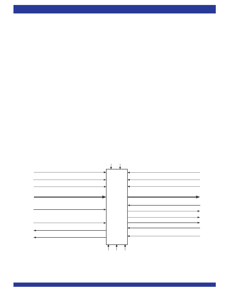
MASTER RESET (MRS)
READ CLOCK (RCLK/RD*)
READ ENABLE (REN)
OUTPUT ENABLE (OE)
EMPTY FLAG/OUTPUT READY (EF/OR)
PROGRAMMABLE ALMOST-EMPTY (PAE)
WRITE CLOCK (WCLK/WR*)
WRITE ENABLE (WEN)
LOAD (LD)
FULL FLAG/INPUT READY (FF/IR)
PROGRAMMABLE ALMOST-FULL (PAF)
PARTIAL RESET (PRS)
FIRST WORD FALL THROUGH/
SERIAL INPUT (FWFT/SI)
RETRANSMIT (RT)
4666 drw03
HALF-FULL FLAG (HF)
SERIAL ENABLE(SEN)
INPUT WIDTH (IW)
OUTPUT WIDTH (OW)
BIG-ENDIAN/LITTLE-ENDIAN (BE)
INTERSPERSED/
NON-INTERSPERSED PARITY (IP)
BUS-
MATCHING
(BM)
(x9 or x18) DATA OUT (Q0 - Qn)
(x9 or x18) DATA IN (D0 - Dn)
IDT
72V223
72V233
72V243
72V253
72V263
72V273
72V283
72V293
Figure 1. Single Device Configuration Signal Flow Diagram
相关PDF资料 |
PDF描述 |
|---|---|
| V300B2M100B | CONVERTER MOD DC/DC 2V 100W |
| MCZ33897TEF | IC TXRX SGL WIRE CAN 14-SOIC |
| IDT72805LB15BG | IC FIFO SYNC DUAL 256X18 121BGA |
| MAX1075ETC+ | IC ADC 10BIT 1.8MSPS 12-TQFN |
| ICL3232EIBNZ-T | IC 2DRVR/2RCVR RS232 3V 16-SOIC |
相关代理商/技术参数 |
参数描述 |
|---|---|
| IDT72V283L15PF | 功能描述:IC FIFO 32768X18 15NS 80QFP RoHS:否 类别:集成电路 (IC) >> 逻辑 - FIFO 系列:72V 标准包装:15 系列:74F 功能:异步 存储容量:256(64 x 4) 数据速率:- 访问时间:- 电源电压:4.5 V ~ 5.5 V 工作温度:0°C ~ 70°C 安装类型:通孔 封装/外壳:24-DIP(0.300",7.62mm) 供应商设备封装:24-PDIP 包装:管件 其它名称:74F433 |
| IDT72V283L15PF8 | 功能描述:IC FIFO 32768X18 15NS 80QFP RoHS:否 类别:集成电路 (IC) >> 逻辑 - FIFO 系列:72V 标准包装:15 系列:74F 功能:异步 存储容量:256(64 x 4) 数据速率:- 访问时间:- 电源电压:4.5 V ~ 5.5 V 工作温度:0°C ~ 70°C 安装类型:通孔 封装/外壳:24-DIP(0.300",7.62mm) 供应商设备封装:24-PDIP 包装:管件 其它名称:74F433 |
| IDT72V283L6BC | 功能描述:IC FIFO 32768X18 6NS 100-BGA RoHS:否 类别:集成电路 (IC) >> 逻辑 - FIFO 系列:72V 标准包装:15 系列:74F 功能:异步 存储容量:256(64 x 4) 数据速率:- 访问时间:- 电源电压:4.5 V ~ 5.5 V 工作温度:0°C ~ 70°C 安装类型:通孔 封装/外壳:24-DIP(0.300",7.62mm) 供应商设备封装:24-PDIP 包装:管件 其它名称:74F433 |
| IDT72V283L6BCG | 制造商:Integrated Device Technology Inc 功能描述:IC FIFO 32768X18 6NS 100-BGA |
| IDT72V283L6PF | 功能描述:IC FIFO 32768X18 6NS 80QFP RoHS:否 类别:集成电路 (IC) >> 逻辑 - FIFO 系列:72V 标准包装:15 系列:74F 功能:异步 存储容量:256(64 x 4) 数据速率:- 访问时间:- 电源电压:4.5 V ~ 5.5 V 工作温度:0°C ~ 70°C 安装类型:通孔 封装/外壳:24-DIP(0.300",7.62mm) 供应商设备封装:24-PDIP 包装:管件 其它名称:74F433 |
发布紧急采购,3分钟左右您将得到回复。