- 您现在的位置:买卖IC网 > PDF目录9935 > IDT72V291L10TFG8 (IDT, Integrated Device Technology Inc)IC FIFO SS 32768X36 10NS 64QFP PDF资料下载
参数资料
| 型号: | IDT72V291L10TFG8 |
| 厂商: | IDT, Integrated Device Technology Inc |
| 文件页数: | 17/26页 |
| 文件大小: | 0K |
| 描述: | IC FIFO SS 32768X36 10NS 64QFP |
| 标准包装: | 1,250 |
| 系列: | 72V |
| 功能: | 同步 |
| 存储容量: | 1.1M(32K x 36) |
| 数据速率: | 100MHz |
| 访问时间: | 10ns |
| 电源电压: | 3 V ~ 3.6 V |
| 工作温度: | 0°C ~ 70°C |
| 安装类型: | 表面贴装 |
| 封装/外壳: | 64-LQFP |
| 供应商设备封装: | 64-TQFP(10x10) |
| 包装: | 带卷 (TR) |
| 其它名称: | 72V291L10TFG8 |
24
COMMERCIAL AND INDUSTRIAL
TEMPERATURE RANGES
IDT72V281/72V291 3.3V CMOS SUPERSYNC FIFOTM
65,536 x 9 and 131,072 x 9
NOTES:
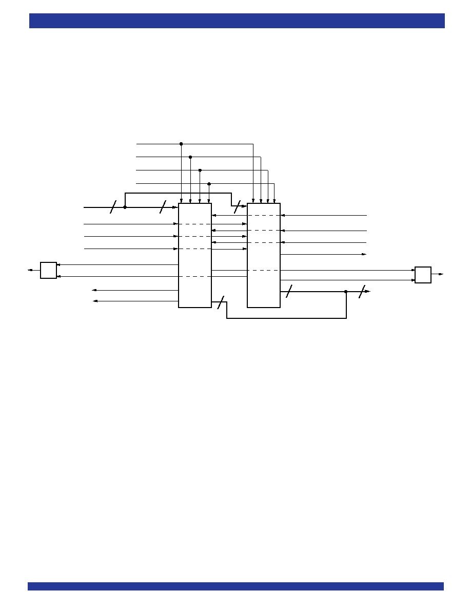
1. Use an AND gate in IDT Standard mode, an OR gate in FWFT mode.
2. Do not connect any output control signals directly together.
3. FIFO #1 and FIFO #2 must be the same depth, but may be different word widths.
OPTIONAL CONFIGURATIONS
WIDTH EXPANSION CONFIGURATION
Word width may be increased simply by connecting together the control
signals of multiple devices. Status flags can be detected from any one
device. The exceptions are the
EF and FF functions in IDT Standard mode
and the
IR and OR functions in FWFT mode. Because of variations in skew
between RCLK and WCLK, it is possible for
EF/FF deassertion and IR/
OR assertion to vary by one cycle between FIFOs. In IDT Standard mode,
Figure 21. Block Diagram of 65,536 x 18 and 131,072 x 18 Width Expansion
DEPTH EXPANSION CONFIGURATION (FWFT MODE ONLY)
The IDT72V281 can easily be adapted to applications requiring depths
greater than 65,536 and 131,072 for the IDT72V291 with a 9-bit bus width.
In FWFT mode, the FIFOs can be connected in series (the data outputs of
one FIFO connected to the data inputs of the next) with no external logic
necessary. The resulting configuration provides a total depth equivalent to
the sum of the depths associated with each single FIFO. Figure 22 shows
a depth expansion using two IDT72V281/72V291 devices.
Care should be taken to select FWFT mode during Master Reset for all
FIFOs in the depth expansion configuration. The first word written to an
empty configuration will pass from one FIFO to the next ("ripple down") until
it finally appears at the outputs of the last FIFO in the chain–no read
operation is necessary but the RCLK of each FIFO must be free-running.
Each time the data word appears at the outputs of one FIFO, that device's
OR line goes LOW, enabling a write to the next FIFO in line.
For an empty expansion configuration, the amount of time it takes for
OR
of the last FIFO in the chain to go LOW (i.e. valid data to appear on the last
FIFO's outputs) after a word has been written to the first FIFO is the sum of the
delays for each individual FIFO:
(N – 1)*(4*transfer clock) + 3*TRCLK
whereNisthenumberofFIFOsintheexpansionandTRCLKistheRCLKperiod.
Note that extra cycles should be added for the possibility that the tSKEW3
specificationisnotmetbetweenWCLKandtransferclock,orRCLKandtransfer
clock, for the
OR flag.
The "ripple down" delay is only noticeable for the first word written to an
empty depth expansion configuration. There will be no delay evident for
subsequent words written to the configuration.
The first free location created by reading from a full depth expansion
configuration will "bubble up" from the last FIFO to the previous one until it
finally moves into the first FIFO of the chain. Each time a free location is
created in one FIFO of the chain, that FIFO's
IR line goes LOW, enabling
the preceding FIFO to write a word to fill it.
such problems can be avoided by creating composite flags, that is, ANDing
EF of every FIFO, and separately ANDing FF of every FIFO. In FWFT
mode, composite flags can be created by ORing
OR of every FIFO, and
separately ORing
IR of every FIFO.
Figure 21 demonstrates a width expansion using two IDT72V281/
72V291 devices. D0 - D8 from each device form a 18-bit wide input bus and
Q0-Q8 from each device form a 18-bit wide output bus. Any word width can
be attained by adding additional IDT72V281/72V291 devices.
WRITE CLOCK (WCLK)
m + n
m
n
MASTER RESET (
MRS)
READ CLOCK (RCLK)
DATA OUT
n
m + n
WRITE ENABLE (
WEN)
FULL FLAG/INPUT READY (
FF/IR)
PROGRAMMABLE (
PAF)
PROGRAMMABLE (
PAE)
EMPTY FLAG/OUTPUT READY (
EF/OR) #2
OUTPUT ENABLE (
OE)
READ ENABLE (
REN)
m
LOAD (
LD)
IDT
72V281
72V291
EMPTY FLAG/OUTPUT READY (
EF/OR) #1
PARTIAL RESET (
PRS)
IDT
72V281
72V291
4513 drw 24
FULL FLAG/INPUT READY (
FF/IR) #2
HALF-FULL FLAG (
HF)
FIRST WORD FALL THROUGH/
SERIAL INPUT (FWFT/SI)
RETRANSMIT (
RT)
#1
FIFO
#2
GATE
(1)
GATE
(1)
D0 - Dm
DATA IN
Dm+1 - Dn
Q0 - Qm
Qm+1 - Qn
FIFO
#1
相关PDF资料 |
PDF描述 |
|---|---|
| VE-241-CU-B1 | CONVERTER MOD DC/DC 12V 200W |
| MS27656E9B35SD | CONN RCPT 6POS WALL MNT W/SCKT |
| VI-25P-CU-B1 | CONVERTER MOD DC/DC 13.8V 200W |
| VI-25M-CU-B1 | CONVERTER MOD DC/DC 10V 200W |
| VI-251-CU-B1 | CONVERTER MOD DC/DC 12V 200W |
相关代理商/技术参数 |
参数描述 |
|---|---|
| IDT72V291L15PF | 功能描述:IC FIFO SS 32768X36 15NS 64QFP RoHS:否 类别:集成电路 (IC) >> 逻辑 - FIFO 系列:72V 标准包装:15 系列:74F 功能:异步 存储容量:256(64 x 4) 数据速率:- 访问时间:- 电源电压:4.5 V ~ 5.5 V 工作温度:0°C ~ 70°C 安装类型:通孔 封装/外壳:24-DIP(0.300",7.62mm) 供应商设备封装:24-PDIP 包装:管件 其它名称:74F433 |
| IDT72V291L15PF8 | 功能描述:IC FIFO SS 32768X36 15NS 64QFP RoHS:否 类别:集成电路 (IC) >> 逻辑 - FIFO 系列:72V 标准包装:15 系列:74F 功能:异步 存储容量:256(64 x 4) 数据速率:- 访问时间:- 电源电压:4.5 V ~ 5.5 V 工作温度:0°C ~ 70°C 安装类型:通孔 封装/外壳:24-DIP(0.300",7.62mm) 供应商设备封装:24-PDIP 包装:管件 其它名称:74F433 |
| IDT72V291L15PFI | 功能描述:IC FIFO SS 32768X36 15NS 64QFP RoHS:否 类别:集成电路 (IC) >> 逻辑 - FIFO 系列:72V 标准包装:15 系列:74F 功能:异步 存储容量:256(64 x 4) 数据速率:- 访问时间:- 电源电压:4.5 V ~ 5.5 V 工作温度:0°C ~ 70°C 安装类型:通孔 封装/外壳:24-DIP(0.300",7.62mm) 供应商设备封装:24-PDIP 包装:管件 其它名称:74F433 |
| IDT72V291L15PFI8 | 功能描述:IC FIFO SS 32768X36 15NS 64QFP RoHS:否 类别:集成电路 (IC) >> 逻辑 - FIFO 系列:72V 标准包装:15 系列:74F 功能:异步 存储容量:256(64 x 4) 数据速率:- 访问时间:- 电源电压:4.5 V ~ 5.5 V 工作温度:0°C ~ 70°C 安装类型:通孔 封装/外壳:24-DIP(0.300",7.62mm) 供应商设备封装:24-PDIP 包装:管件 其它名称:74F433 |
| IDT72V291L15TF | 功能描述:IC FIFO SS 32768X36 15NS 64QFP RoHS:否 类别:集成电路 (IC) >> 逻辑 - FIFO 系列:72V 标准包装:15 系列:74F 功能:异步 存储容量:256(64 x 4) 数据速率:- 访问时间:- 电源电压:4.5 V ~ 5.5 V 工作温度:0°C ~ 70°C 安装类型:通孔 封装/外壳:24-DIP(0.300",7.62mm) 供应商设备封装:24-PDIP 包装:管件 其它名称:74F433 |
发布紧急采购,3分钟左右您将得到回复。