- 您现在的位置:买卖IC网 > PDF目录9185 > IDT72V73273BB (IDT, Integrated Device Technology Inc)IC DGTL SW 32768X32768 208-BGA PDF资料下载
参数资料
| 型号: | IDT72V73273BB |
| 厂商: | IDT, Integrated Device Technology Inc |
| 文件页数: | 23/36页 |
| 文件大小: | 0K |
| 描述: | IC DGTL SW 32768X32768 208-BGA |
| 标准包装: | 12 |
| 系列: | 72V |
| 类型: | 多路复用器 |
| 电路: | 8 x 1:1 |
| 电压电源: | 单电源 |
| 电源电压: | 3 V ~ 3.6 V |
| 工作温度: | -40°C ~ 85°C |
| 安装类型: | 表面贴装 |
| 封装/外壳: | 208-BGA |
| 供应商设备封装: | 208-PBGA(17x17) |
| 包装: | 托盘 |
| 其它名称: | 72V73273BB |
第1页第2页第3页第4页第5页第6页第7页第8页第9页第10页第11页第12页第13页第14页第15页第16页第17页第18页第19页第20页第21页第22页当前第23页第24页第25页第26页第27页第28页第29页第30页第31页第32页第33页第34页第35页第36页
3
INDUSTRIAL TEMPERATURERANGE
IDT72V73273 3.3V TIME SLOT INTERCHANGE
DIGITAL SWITCH WITH RATE MATCHING 32,768 x 32,768 CHANNELS
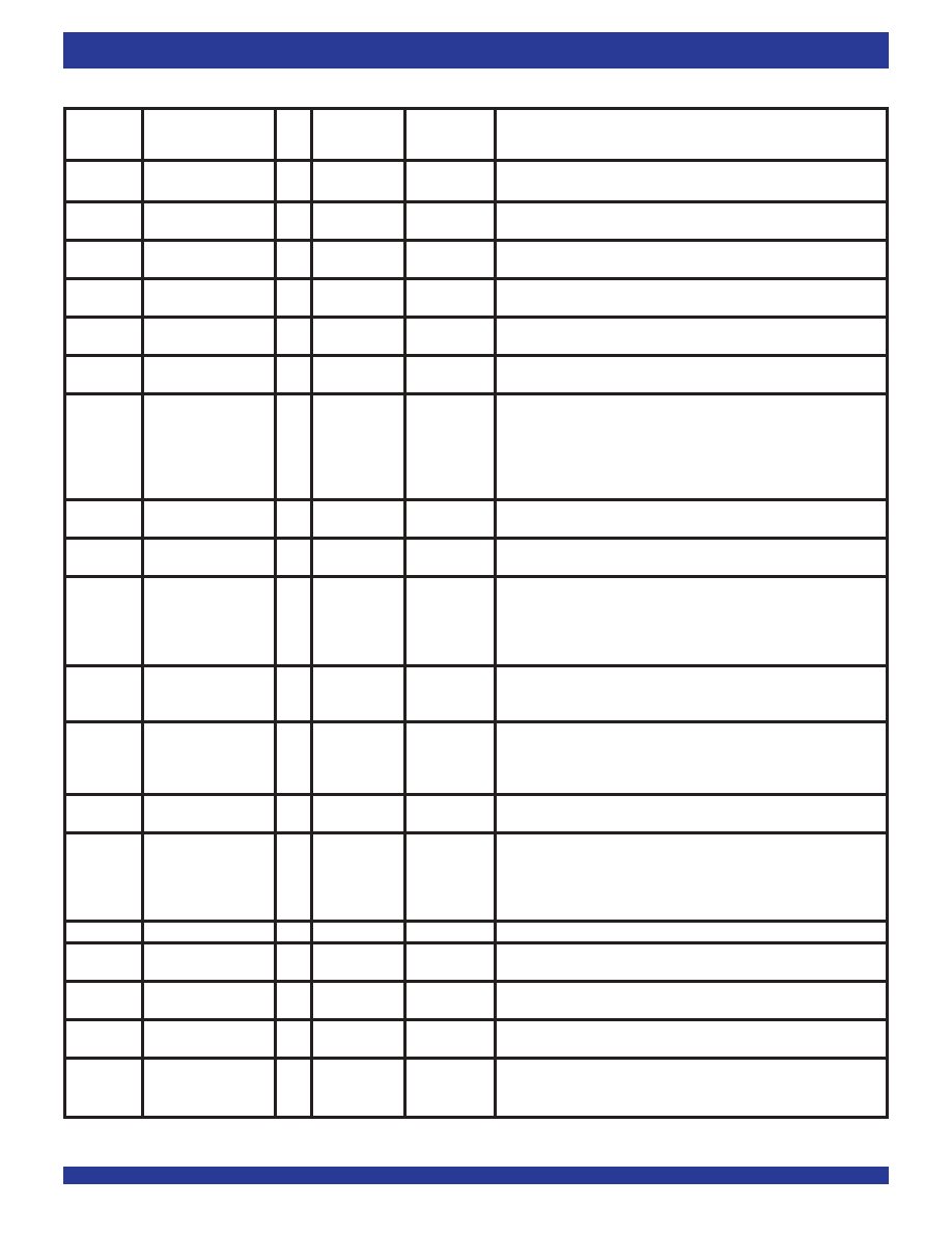
PIN DESCRIPTION
A0-A15
Address0-15
I
*See PQFP
*See PBGA
Theseaddresslinesaccessallinternalmemories.
TableBelow
BEL
Byte Enable LOW
I
31
L4
In synchronous mode, this input will enable the lower byte (D0-7) on to the data
bus.
C32i
Clock
I
2
A1
Serialclockforshiftingdatain/outontheserialdatastreams. Thisinputaccepts
a 32.768MHz clock.
CS
Chip Select
I
12
E1
Active LOW input used by a microprocessor to activate the microprocessor port
of the device.
D0-15
DataBus0-15
I/O
*See PQFP
*See PBGA
Thesepinsarethedatabusofthemicroprocessorport.
TableBelow
DS
DataStrobe
I
11
D4
This active LOW input works in conjunction with CS to enable the read and write
operations. ThisactiveLOWinputsetsthedatabuslines(D0-D15).
DTA/BEH
DataTransfer
I/O
32
K2
Inasynchronousmodethispinindicatesthatadatabustransferiscomplete.
Acknowledgment
When the bus cycle ends, this pin drives HIGH and then High-Z allowing for
Active LOW Output
faster bus cycles with a weaker pull-up resistor. A pull-up resistor is required to
/Byte Enable HIGH
hold a HIGH level when the pin is High-Z. When the device is in
synchronous bus mode, this pin acts as an input and will enable the upper byte
(D8-15)ontothedatabus.
F32i
FramePulse
I
3
B1
Thisinputacceptsandautomaticallyidentifiesframesynchronizationsignals
formattedaccordingtoST-BUS andGCIspecifications.
GND
*See PQFP
*See PBGA
Ground.
TableBelow
ODE
OutputDriveEnable
I
207
A3
ThisistheoutputenablecontrolfortheTXserialoutputs.WhenODEinputis
LOW and the OSB bit of the CR register is LOW, all TX outputs are in a High-
Impedance state. If this input is HIGH, the TX outputdriversareenabled.
However, each channel may still be put into a High-Impedance state by using
the per channel control bits in the Connection Memory HIGH.
RX0-63
RX Input 0 to 63
I
*See PQFP
*See PBGA
Serial data Input Stream. These streams may have data rates of 2.048Mb/s,
TableBelow
4.096Mb/s,8.192Mb/s,16.384Mb/s,or32.768Mb/sdependinguponthe
selectioninReceiveDataRateSelectionRegister(RDRSR).
RESET
Device Reset:
I
208
A2
This input (active LOW) puts the device in its reset state that clears the device
internalcounters,registersandbringsTX0-63andmicroportdataoutputstoa
High-Impedance state. The RESET pin must be held LOW for a minimum of
20ns to reset the device.
R/W
Read/Write
I
13
E2
Thisinputcontrolsthedirectionofthedatabuslines(D0-D15)duringa
microprocessoraccess.
S/A
Synchronous/
I
5
C1
Thisinputwillselectbetweenasynchronousmicroprocessorbustimingand
Asynchronous
synchronous microprocessor bus timing. In synchronous mode, DTA/BEH
Bus Mode
acts as the BEH input and is used in conjunction with BEL to output data on the
data bus. In asynchronous bus mode, BEL is tied LOW and DTA/BEH acts as
theDTA,databusacknowledgmentoutput.
TCK
Test Clock
I
9
D2
Provides the clock to the JTAG test logic.
TDI
Test Serial Data In
I
7
C3
JTAG serial test instructions and data are shifted in on this pin. This pin is pulled
HIGH by an internal pull-up when not driven.
TDO
TestSerialDataOut
O
8
D1
JTAG serial data is output on this pin on the falling edge of TCK. This pin is held i
in High-Impedance state when JTAG scan is not enabled.
TMS
TestModeSelect
I
6
C2
JTAGsignalthatcontrolsthestatetransitionsoftheTAPcontroller.Thispinis
pulled HIGH by an internal pull-up when not driven.
TRST
TestReset
I
10
D3
Asynchronously initializes the JTAG TAP controller by putting it in the Test-
Logic-Resetstate.Thispinispulledbyaninternalpull-upwhennotdriven.This
pin should be pulsed LOW on power-up, or held LOW, to ensure that the device
SYMBOL
NAME
I/O
PQFP
PBGA
DESCRIPTION
PIN NO.
相关PDF资料 |
PDF描述 |
|---|---|
| MAX5387LAUD+T | IC DGTL POT 256POS 10K 14TSSOP |
| M83723/76R22129 | CONN PLUG 12POS STRAIGHT W/PINS |
| MAX5386NATE+T | IC DGTL POT 256TAP DUAL 16-TQFN |
| VI-BWY-MX-F2 | CONVERTER MOD DC/DC 3.3V 49.5W |
| VI-BWY-MX-F1 | CONVERTER MOD DC/DC 3.3V 49.5W |
相关代理商/技术参数 |
参数描述 |
|---|---|
| IDT72V73273BBG | 功能描述:IC DGTL SW 32768X32768 208-BGA RoHS:是 类别:集成电路 (IC) >> 逻辑 - 信号开关,多路复用器,解码器 系列:72V 标准包装:48 系列:74VHC 类型:多路复用器 电路:4 x 2:1 独立电路:1 输出电流高,低:8mA,8mA 电压电源:单电源 电源电压:2 V ~ 5.5 V 工作温度:-40°C ~ 85°C 安装类型:表面贴装 封装/外壳:16-SOIC(0.154",3.90mm 宽) 供应商设备封装:16-SOIC 包装:管件 |
| IDT72V801L10PF | 功能描述:IC SYNC FIFO 256X9 10NS 64QFP RoHS:否 类别:集成电路 (IC) >> 逻辑 - FIFO 系列:72V 标准包装:90 系列:7200 功能:同步 存储容量:288K(16K x 18) 数据速率:100MHz 访问时间:10ns 电源电压:4.5 V ~ 5.5 V 工作温度:0°C ~ 70°C 安装类型:表面贴装 封装/外壳:64-LQFP 供应商设备封装:64-TQFP(14x14) 包装:托盘 其它名称:72271LA10PF |
| IDT72V801L10PF8 | 功能描述:IC SYNC FIFO 256X9 10NS 64QFP RoHS:否 类别:集成电路 (IC) >> 逻辑 - FIFO 系列:72V 标准包装:90 系列:7200 功能:同步 存储容量:288K(16K x 18) 数据速率:100MHz 访问时间:10ns 电源电压:4.5 V ~ 5.5 V 工作温度:0°C ~ 70°C 安装类型:表面贴装 封装/外壳:64-LQFP 供应商设备封装:64-TQFP(14x14) 包装:托盘 其它名称:72271LA10PF |
| IDT72V801L10PFG | 功能描述:IC FIFO 256X9 SYNC DUAL 64TQFP RoHS:是 类别:集成电路 (IC) >> 逻辑 - FIFO 系列:72V 标准包装:90 系列:7200 功能:同步 存储容量:288K(16K x 18) 数据速率:100MHz 访问时间:10ns 电源电压:4.5 V ~ 5.5 V 工作温度:0°C ~ 70°C 安装类型:表面贴装 封装/外壳:64-LQFP 供应商设备封装:64-TQFP(14x14) 包装:托盘 其它名称:72271LA10PF |
| IDT72V801L10PFG8 | 制造商:Integrated Device Technology Inc 功能描述:IC SYNC FIFO 256X9 10NS 64QFP |
发布紧急采购,3分钟左右您将得到回复。