- 您现在的位置:买卖IC网 > PDF目录9185 > IDT72V73273BB (IDT, Integrated Device Technology Inc)IC DGTL SW 32768X32768 208-BGA PDF资料下载
参数资料
| 型号: | IDT72V73273BB |
| 厂商: | IDT, Integrated Device Technology Inc |
| 文件页数: | 35/36页 |
| 文件大小: | 0K |
| 描述: | IC DGTL SW 32768X32768 208-BGA |
| 标准包装: | 12 |
| 系列: | 72V |
| 类型: | 多路复用器 |
| 电路: | 8 x 1:1 |
| 电压电源: | 单电源 |
| 电源电压: | 3 V ~ 3.6 V |
| 工作温度: | -40°C ~ 85°C |
| 安装类型: | 表面贴装 |
| 封装/外壳: | 208-BGA |
| 供应商设备封装: | 208-PBGA(17x17) |
| 包装: | 托盘 |
| 其它名称: | 72V73273BB |
第1页第2页第3页第4页第5页第6页第7页第8页第9页第10页第11页第12页第13页第14页第15页第16页第17页第18页第19页第20页第21页第22页第23页第24页第25页第26页第27页第28页第29页第30页第31页第32页第33页第34页当前第35页第36页
8
INDUSTRIAL TEMPERATURERANGE
IDT72V73273 3.3V TIME SLOT INTERCHANGE
DIGITAL SWITCH WITH RATE MATCHING 32,768 x 32,768 CHANNELS
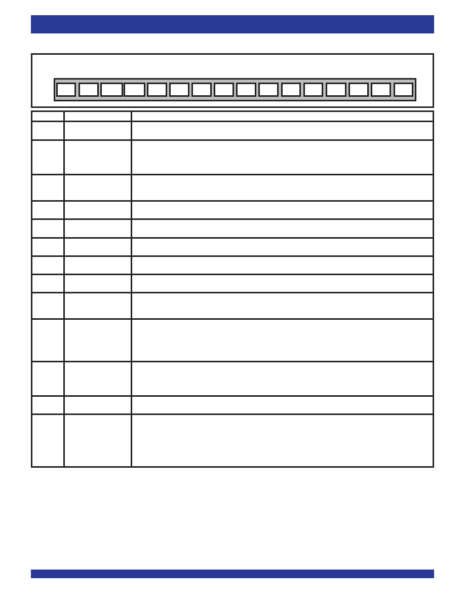
TABLE 3 CONTROL REGISTER (CR) BITS
Reset Value:
0000H
15
14
13
12
11
10
987654
32
1
0
BIT
NAME
DESCRIPTION
15
SRS
A one will reset the device and have the same effect as the RESET pin. Must be zero for normal operation.
(SoftwareReset)
14
BYP
WhentheBypassbitis1,allRXstreamswillbe“shorted”toTX--ineffectbypassingallinternalcircuitryoftheTSI.Thiseffectively
(RX/TXBypass)
setstheTSItoa1-to-1switchmodewithalmostonlyafewnanosecondsofdelay. Azerocanbewrittentoallownormaloperation.
TheintentionofthismodeistominimizethedelayfromtheRXinputtotheTXoutputmakingtheTSI“invisible”. Anyoffsetvalues
in the FOR register will be required.
13
OEPOL
When 1, a one on OEI pin denotes an active state on the output data stream; zero on OEI pin denotes High-Impedance state.
(OutputEnablePolarity)
When 0, a one denotes High-Impedance and a zero denotes an active state. OEI mode is entered on a per-group basis in the
DRSR.
12
AOE
When1,alloutputstreampin(TXn)becomeOEItoallowforatwo-chipsolutionforalargerswitchingmatrixwithOEIpins.When
(AllOutputEnable)
in AOE the DRS must be set to the corresponding data rates of the other device.
11
PRST
When HIGH, the PRBS transmitter output will be initialized.
(PRBS Reset)
10
CBER
A low to high transition of this bit clears the BER register (BERR).
(Clear Bit Error Rate)
9
SBER
A low to high transition in this bit starts the bit error rate test. The bit error test result is kept in the BER register (BERR).
(StartBitErrorRate)
8
FBP
When 1, this bit overrides the BPSA and BPEA registers and programs the full Connection Memory space. When 0, the BPSA
(FullBlockProgramming)
and BPEAdetermine the Connection Memory space to be programmed.
7-5
BPD2-0
ThesebitscarrythevaluetobeloadedintotheConnectionMemoryblockwhenevertheConnectionMemoryblockprogramming
(BlockProgrammingData) feature is activated. After the BPE bit is set to 1 from 0, the contents of the bits BPD2-0 are loaded into bit 2, 1 and 0 (MOD2-0)
of the Connection Memory HIGH.
4
BPE
AzerotoonetransitionofthisbitenablestheConnectionMemoryblockprogrammingfeaturedelimitedbytheBPSAandBPEA
(Begin Block
registersaswellasforafullbackprogram.OncetheBPEbitissetHIGH,thedevicewillprogramtheConnection Memoryblock
ProgrammingEnable)
asfastas thaniftheusermanuallyprogrammedeachConnectionMemorylocationthroughthemicroprocessor. Aftertheprogramming
functionhasfinished,theBPEbitreturnstozerotoindicatetheoperationhascompleted. WhentheBPE=1,theBPEbitcan be
setto0toabortblockprogramming.
3
RCML
When RCML =1, all bits 14-0 in Connection Memory LOW will be reset to zero during block programming; when RCML=0,
(ResetConnection
bits 14-0 in Connection Memory LOW will retain their original values during block programming.
Memory LOW in Block
`
Programming)
2
OSB
When ODE = 0 and OSB = 0, the output drivers of transmit serial streams are in High-Impedance mode. When either ODE = 1
(OutputStandby)
or OSB = 1, the output serial stream drivers function normally.
1-0
MS1-0
These two bits decide which memory to be accessed via microprocessor port.
(Memory Select)
00 -- Connection Memory LOW
01 -- Connection Memory HIGH
10 -- Data Memory
11 -- Reserved
SRS
BYP
OEPOL
AOE
PRST
CBER
SBER
FBP
BPD2
BPD1
BPD0
BPE
RCML
OSB
MS1
MS0
相关PDF资料 |
PDF描述 |
|---|---|
| MAX5387LAUD+T | IC DGTL POT 256POS 10K 14TSSOP |
| M83723/76R22129 | CONN PLUG 12POS STRAIGHT W/PINS |
| MAX5386NATE+T | IC DGTL POT 256TAP DUAL 16-TQFN |
| VI-BWY-MX-F2 | CONVERTER MOD DC/DC 3.3V 49.5W |
| VI-BWY-MX-F1 | CONVERTER MOD DC/DC 3.3V 49.5W |
相关代理商/技术参数 |
参数描述 |
|---|---|
| IDT72V73273BBG | 功能描述:IC DGTL SW 32768X32768 208-BGA RoHS:是 类别:集成电路 (IC) >> 逻辑 - 信号开关,多路复用器,解码器 系列:72V 标准包装:48 系列:74VHC 类型:多路复用器 电路:4 x 2:1 独立电路:1 输出电流高,低:8mA,8mA 电压电源:单电源 电源电压:2 V ~ 5.5 V 工作温度:-40°C ~ 85°C 安装类型:表面贴装 封装/外壳:16-SOIC(0.154",3.90mm 宽) 供应商设备封装:16-SOIC 包装:管件 |
| IDT72V801L10PF | 功能描述:IC SYNC FIFO 256X9 10NS 64QFP RoHS:否 类别:集成电路 (IC) >> 逻辑 - FIFO 系列:72V 标准包装:90 系列:7200 功能:同步 存储容量:288K(16K x 18) 数据速率:100MHz 访问时间:10ns 电源电压:4.5 V ~ 5.5 V 工作温度:0°C ~ 70°C 安装类型:表面贴装 封装/外壳:64-LQFP 供应商设备封装:64-TQFP(14x14) 包装:托盘 其它名称:72271LA10PF |
| IDT72V801L10PF8 | 功能描述:IC SYNC FIFO 256X9 10NS 64QFP RoHS:否 类别:集成电路 (IC) >> 逻辑 - FIFO 系列:72V 标准包装:90 系列:7200 功能:同步 存储容量:288K(16K x 18) 数据速率:100MHz 访问时间:10ns 电源电压:4.5 V ~ 5.5 V 工作温度:0°C ~ 70°C 安装类型:表面贴装 封装/外壳:64-LQFP 供应商设备封装:64-TQFP(14x14) 包装:托盘 其它名称:72271LA10PF |
| IDT72V801L10PFG | 功能描述:IC FIFO 256X9 SYNC DUAL 64TQFP RoHS:是 类别:集成电路 (IC) >> 逻辑 - FIFO 系列:72V 标准包装:90 系列:7200 功能:同步 存储容量:288K(16K x 18) 数据速率:100MHz 访问时间:10ns 电源电压:4.5 V ~ 5.5 V 工作温度:0°C ~ 70°C 安装类型:表面贴装 封装/外壳:64-LQFP 供应商设备封装:64-TQFP(14x14) 包装:托盘 其它名称:72271LA10PF |
| IDT72V801L10PFG8 | 制造商:Integrated Device Technology Inc 功能描述:IC SYNC FIFO 256X9 10NS 64QFP |
发布紧急采购,3分钟左右您将得到回复。