- 您现在的位置:买卖IC网 > PDF目录10047 > IDT72V801L20PF (IDT, Integrated Device Technology Inc)IC SYNC FIFO 256X9 20NS 64QFP PDF资料下载
参数资料
| 型号: | IDT72V801L20PF |
| 厂商: | IDT, Integrated Device Technology Inc |
| 文件页数: | 1/16页 |
| 文件大小: | 0K |
| 描述: | IC SYNC FIFO 256X9 20NS 64QFP |
| 标准包装: | 90 |
| 系列: | 72V |
| 功能: | 异步 |
| 存储容量: | 2.3K(256 x 9) |
| 数据速率: | 50MHz |
| 访问时间: | 20ns |
| 电源电压: | 3 V ~ 3.6 V |
| 工作温度: | 0°C ~ 70°C |
| 安装类型: | 表面贴装 |
| 封装/外壳: | 64-LQFP |
| 供应商设备封装: | 64-TQFP(14x14) |
| 包装: | 托盘 |
| 其它名称: | 72V801L20PF |
1
COMMERCIAL AND INDUSTRIAL TEMPERATURE RANGES
3.3 VOLT DUAL CMOS SyncFIFO
DUAL 256 X 9, DUAL 512 X 9,
DUAL 1,024 X 9, DUAL 2,048 X 9,
DUAL 4,096 X 9 , DUAL 8,192 X 9
IDT72V801
IDT72V811
IDT72V821
IDT72V831
IDT72V841
IDT72V851
OCTOBER 2008
IDT and the IDT logo are registered trademarks of Integrated Device Technology, Inc. The TeraSync FIFO is a trademark of Integrated Device Technology, Inc.
2008 Integrated Device Technology, Inc. All rights reserved. Product specifications subject to change without notice.
DSC-4093/4
FEATURES:
The IDT72V801 is equivalent to two IDT72V201 256 x 9 FIFOs
The IDT72V811 is equivalent to two IDT72V211 512 x 9 FIFOs
The IDT72V821 is equivalent to two IDT72V221 1,024 x 9 FIFOs
The IDT72V831 is equivalent to two IDT72V231 2,048 x 9 FIFOs
The IDT72V841 is equivalent to two IDT72V241 4,096 x 9 FIFOs
The IDT72V851 is equivalent to two IDT72V251 8,192 x 9 FIFOs
Offers optimal combination of large capacity, high speed,
design flexibility and small footprint
Ideal for prioritization, bidirectional, and width expansion
applications
10 ns read/write cycle time
5V input tolerant
Separate control lines and data lines for each FIFO
Separate Empty, Full, programmable Almost-Empty and
Almost-Full flags for each FIFO
Enable puts output data lines in high-impedance state
Space-saving 64-pin plastic Thin Quad Flat Pack (TQFP/
STQFP)
Industrial temperature range (–40
°°°°°C to +85°°°°°C) is available
Green parts available, see ordering information
DESCRIPTION:
The IDT72V801/72V811/72V821/72V831/72V841/72V851/72V851 are
dual synchronous (clocked) FIFOs. The device is functionally equivalent to
two IDT72V201/72V211/72V221/72V231/72V241/72V251 FIFOs in a single
package with all associated control, data, and flag lines assigned to separate
pins.
Each of the two FIFOs (designated FIFO A and FIFO B) contained in the
IDT72V801/72V811/72V821/72V831/72V841/72V851 has a 9-bit input data
port (DA0 - DA8, DB0 - DB8) and a 9-bit output data port (QA0 - QA8,
QB0 - QB8). Each input port is controlled by a free-running clock (WCLKA,
WCLKB), and two Write Enable pins (
WENA1, WENA2, WENB1, WENB2).
DataiswrittenintoeachofthetwoarraysoneveryrisingclockedgeoftheWrite
Clock (WCLKA, WCLKB) when the appropriate Write Enable pins are
asserted.
The output port of each FIFO bank is controlled by its associated clock pin
(RCLKA, RCLKB) and two Read Enable pins (
RENA1, RENA2, RENB1,
RENB2).TheReadClockcanbetiedtotheWriteClockforsingleclockoperation
orthetwoclockscanrunasynchronousofoneanotherfordualclockoperation.
An Output Enable pin (
OEA, OEB) is provided on the read port of each FIFO
for three-state output control.
Each of the two FIFOs has two fixed flags, Empty (
EFA,EFB)andFull(FFA,
FFB). Twoprogrammableflags,Almost-Empty(PAEA,PAEB)andAlmost-Full
(
PAFA,PAFB),areprovidedforeachFIFObanktoimprovememoryutilization.
If not programmed, the programmable flags default to Empty+7 for
PAEAand
PAEB, and Full-7 for PAFA and PAFB.
The IDT72V801/72V811/72V821/72V831/72V841/72V851 architecture
lends itself to many flexible configurations such as:
2-level priority data buffering
Bidirectional operation
Width expansion
Depth expansion
This FIFO is fabricated using IDT's high-performance submicron CMOS
technology.
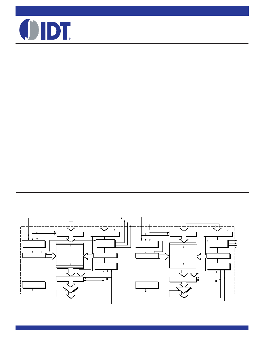
FUNCTIONAL BLOCK DIAGRAM
WCLKA
WENA1
WENA2
DA0 - DA8
LDA
OFFSET REGISTER
INPUT REGISTER
WRITE CONTROL
LOGIC
RESET LOGIC
OUTPUT REGISTER
OEA
RSA
QA0 - QA8
RCLKA
RENA1
RENA2
READ CONTROL
LOGIC
READ POINTER
FLAG
LOGIC
EFA
PAEA
PAFA
FFA
4093 drw 01
WCLKB
WENB1
WENB2
DB0 - DB8
LDB
OFFSET REGISTER
INPUT REGISTER
RAM ARRAY
256 x 9, 512 x 9,
1,024 x 9, 2,048 x 9,
4,096 x 9, 8,192 x 9
WRITE CONTROL
LOGIC
WRITE POINTER
RESET LOGIC
OUTPUT REGISTER
OEB
RSB
QB0 - QB8
RCLKB
RENB1
RENB2
READ CONTROL
LOGIC
READ POINTER
FLAG
LOGIC
EFB
PAFB
FFB
PAEB
WRITE POINTER
RAM ARRAY
256 x 9, 512 x 9,
1,024 x 9, 2,048 x 9,
4,096 x 9, 8,192 x 9
相关PDF资料 |
PDF描述 |
|---|---|
| MS27467T21A41S | CONN PLUG 41POS STRAIGHT W/SCKT |
| D38999/20FG39PD | CONN RCPT 39POS WALL MNT W/PINS |
| MS27466E13A98P | CONN RCPT 10POS WALL MT W/PINS |
| IDT72V801L20TF | IC SYNC FIFO 256X9 20NS 64QFP |
| MS27473T20A35PB | CONN PLUG 79POS STRAIGHT W/PINS |
相关代理商/技术参数 |
参数描述 |
|---|---|
| IDT72V801L20PF8 | 功能描述:IC SYNC FIFO 256X9 20NS 64QFP RoHS:否 类别:集成电路 (IC) >> 逻辑 - FIFO 系列:72V 标准包装:80 系列:7200 功能:同步 存储容量:18.4K(1K x 18) 数据速率:- 访问时间:10ns 电源电压:4.5 V ~ 5.5 V 工作温度:0°C ~ 70°C 安装类型:表面贴装 封装/外壳:64-LQFP 供应商设备封装:64-TQFP(10x10) 包装:托盘 其它名称:72225LB10TF |
| IDT72V801L20TF | 功能描述:IC SYNC FIFO 256X9 20NS 64QFP RoHS:否 类别:集成电路 (IC) >> 逻辑 - FIFO 系列:72V 标准包装:90 系列:7200 功能:同步 存储容量:288K(16K x 18) 数据速率:100MHz 访问时间:10ns 电源电压:4.5 V ~ 5.5 V 工作温度:0°C ~ 70°C 安装类型:表面贴装 封装/外壳:64-LQFP 供应商设备封装:64-TQFP(14x14) 包装:托盘 其它名称:72271LA10PF |
| IDT72V801L20TF8 | 功能描述:IC SYNC FIFO 256X9 20NS 64QFP RoHS:否 类别:集成电路 (IC) >> 逻辑 - FIFO 系列:72V 标准包装:80 系列:7200 功能:同步 存储容量:18.4K(1K x 18) 数据速率:- 访问时间:10ns 电源电压:4.5 V ~ 5.5 V 工作温度:0°C ~ 70°C 安装类型:表面贴装 封装/外壳:64-LQFP 供应商设备封装:64-TQFP(10x10) 包装:托盘 其它名称:72225LB10TF |
| IDT72V805L10PF | 功能描述:IC FIFO SYNC 256X18 10NS 128QFP RoHS:否 类别:集成电路 (IC) >> 逻辑 - FIFO 系列:72V 标准包装:90 系列:7200 功能:同步 存储容量:288K(16K x 18) 数据速率:100MHz 访问时间:10ns 电源电压:4.5 V ~ 5.5 V 工作温度:0°C ~ 70°C 安装类型:表面贴装 封装/外壳:64-LQFP 供应商设备封装:64-TQFP(14x14) 包装:托盘 其它名称:72271LA10PF |
| IDT72V805L10PF8 | 功能描述:IC FIFO SYNC 256X18 10NS 128QFP RoHS:否 类别:集成电路 (IC) >> 逻辑 - FIFO 系列:72V 标准包装:90 系列:7200 功能:同步 存储容量:288K(16K x 18) 数据速率:100MHz 访问时间:10ns 电源电压:4.5 V ~ 5.5 V 工作温度:0°C ~ 70°C 安装类型:表面贴装 封装/外壳:64-LQFP 供应商设备封装:64-TQFP(14x14) 包装:托盘 其它名称:72271LA10PF |
发布紧急采购,3分钟左右您将得到回复。