- 您现在的位置:买卖IC网 > PDF目录10037 > IDT72V805L20PF (IDT, Integrated Device Technology Inc)IC FIFO SYNC 256X18 20NS 128QFP PDF资料下载
参数资料
| 型号: | IDT72V805L20PF |
| 厂商: | IDT, Integrated Device Technology Inc |
| 文件页数: | 12/26页 |
| 文件大小: | 0K |
| 描述: | IC FIFO SYNC 256X18 20NS 128QFP |
| 标准包装: | 72 |
| 系列: | 72V |
| 功能: | 异步,同步 |
| 存储容量: | 4.6K(256 x 18) |
| 数据速率: | 50MHz |
| 访问时间: | 20ns |
| 电源电压: | 3 V ~ 3.6 V |
| 工作温度: | 0°C ~ 70°C |
| 安装类型: | 表面贴装 |
| 封装/外壳: | 128-LQFP |
| 供应商设备封装: | 128-TQFP(14x20) |
| 包装: | 托盘 |
| 其它名称: | 72V805L20PF |
2
IDT72V805/72V815/72V825/72V835/72V845
3.3 V CMOS DUAL SyncFIFO 256 x 18, 512 x 18, 1,024 x 18, 4,096 x 18
COMMERCIAL AND INDUSTRIAL
TEMPERATURE RANGES
FEBRUARY 11, 2009
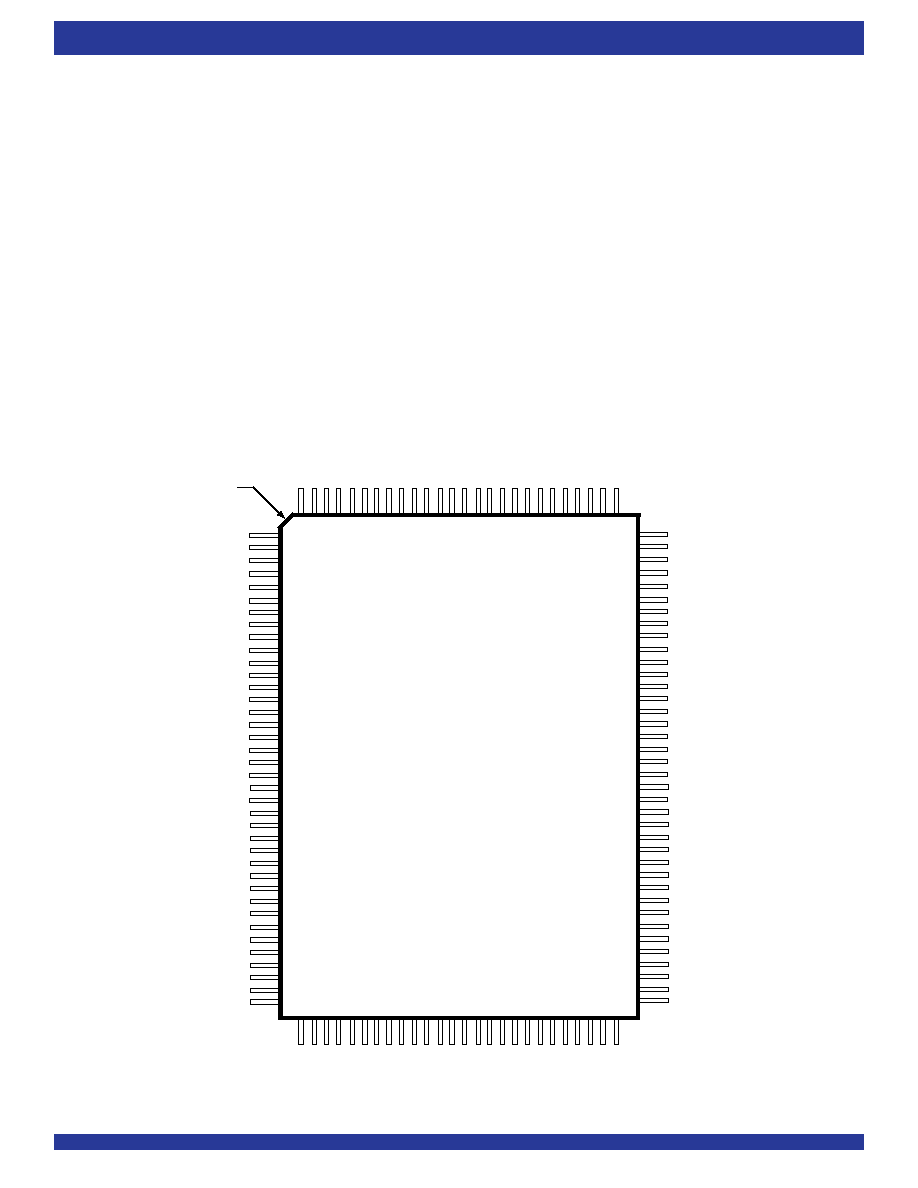
PIN CONFIGURATIONS
TQFP (PK128-1, ORDER CODE: PF)
TOP VIEW
First-Out (FIFO) memories with clocked read and write controls. These FIFOs
are applicable for a wide variety of data buffering needs, such as optical disk
controllers, Local Area Networks (LANs), and interprocessor communication.
Each of the two FIFOs contained in these devices has an 18-bit input and
output port. Each input port is controlled by a free-running clock (WCLK), and
an input enable pin (
WEN). Data is read into the synchronous FIFO on every
clock when
WEN isasserted.TheoutputportofeachFIFObankiscontrolled
by another clock pin (RCLK) and another enable pin (
REN). The Read Clock
can be tied to the Write Clock for single clock operation or the two clocks can
run asynchronous of one another for dual-clock operation. An Output Enable
pin (
OE) is provided on the read port of each FIFO for three-state control of
the output.
The synchronous FIFOs have two fixed flags, Empty Flag/Output Ready
(
EF/OR) and Full Flag/Input Ready (FF/IR), and two programmable flags,
Almost-Empty (
PAE) and Almost-Full (PAF). The offset loading of the
programmable flags is controlled by a simple state machine, and is initiated
by asserting the Load pin (
LD). AHalf-Fullflag(HF)isavailableforeachFIFO
that is implemented as a single device.
There are two possible timing modes of operation with these devices:
IDT Standard mode and First Word Fall Through (FWFT) mode.
In IDT Standard Mode, the first word written to an empty FIFO will not
appear on the data output lines unless a specific read operation is
performed. A read operation, which consists of activating
REN and
enabling a rising RCLK edge, will shift the word from internal memory to the
data output lines.
In FWFT mode, the first word written to an empty FIFO is clocked directly
to the data output lines after three transitions of the RCLK signal. A
REN
does not have to be asserted for accessing the first word.
These devices are depth expandable using a Daisy-Chain technique or
First Word Fall Through (FWFT) mode. The
XI and XO pins are used to
expand the FIFOs. In depth expansion configuration,
FL is grounded on
the first device and set to HIGH for all other devices in the Daisy Chain.
The IDT72V805/72V815/72V825/72V835/72V845 are fabricated using
IDT’s high-speed submicron CMOS technology.
VCC
LDA
1
2
3
4
5
6
7
8
9
10
11
12
13
14
15
16
17
18
19
20
21
22
23
24
25
26
27
28
29
30
31
32
33
34
35
36
37
38
PAFA
RXIA
FFA
WXOA/HFA
RXOA
QA0
QA1
GND
QA2
QA3
VCC
QA4
GND
QA5
QA6
QA7
QA8
GND
DB7
DB6
DB5
DB4
DB3
DB2
DB1
DB0
PAEB
FLB
WCLKB
WENB
WXIB
VCC
PAFB
RXIB
FFB
WXOB/HFB
RXOB
39
40
41
42
43
44
45
46
47
48
49
50
51
52
53
54
55
56
57
58
59
60
61
62
63
64
65
66
67
68
69
70
71
72
73
74
75
76
77
78
79
80
81
82
83
84
85
86
87
88
89
90
91
92
93
94
95
96
97
98
99
100
102
101
128
127
126
125
124
123
122
121
120
119
118
117
116
115
114
113
112
111
110
109
108
107
106
105
OEA
RSA
VCC
GND
EFA
QA17
QA16
GND
QA15
VCC
QA14
QA13
GND
QA12
QA11
VCC
QA10
QA9
DB8
DB9
DB10
DB11
DB12
DB13
DB14
DB15
DB16
DB17
RCLKB
RENB
LDB
OEB
RSB
VCC
GND
EFB
WXIA
WENA
WCLKA
FLA
PAEA
DA0
DA1
DA2
DA3
DA4
DA5
DA6
DA7
DA8
DA9
DA10
DA11
DA12
DA13
DA14
DA16
DA17
GND
RCLKA
RENA
QB0
QB1
GND
Q
B
2
QB3
V
CC
QB4
GND
QB5
QB6
QB7
QB8
GND
QB9
QB10
V
CC
QB11
QB12
GND
QB13
QB14
V
CC
QB15
GND
QB16
Q
B
1
7
104
103
INDEX
GND
DA15
4295 drw 02
DESCRIPTION (CONTINUED)
相关PDF资料 |
PDF描述 |
|---|---|
| VI-BTH-MY | CONVERTER MOD DC/DC 52V 50W |
| LTC1322CSW#TR | IC TXRX RS232/485/EIA562 24SOIC |
| AD7572LN05 | IC ADC 12BIT HS LC2MOS 24-DIP |
| LTC1348ISW#TRPBF | IC TXRX 3.3V/5V RS232 28-SOIC |
| VI-J04-MX-S | CONVERTER MOD DC/DC 48V 75W |
相关代理商/技术参数 |
参数描述 |
|---|---|
| IDT72V805L20PF8 | 功能描述:IC FIFO SYNC 256X18 20NS 128QFP RoHS:否 类别:集成电路 (IC) >> 逻辑 - FIFO 系列:72V 标准包装:80 系列:7200 功能:同步 存储容量:18.4K(1K x 18) 数据速率:- 访问时间:10ns 电源电压:4.5 V ~ 5.5 V 工作温度:0°C ~ 70°C 安装类型:表面贴装 封装/外壳:64-LQFP 供应商设备封装:64-TQFP(10x10) 包装:托盘 其它名称:72225LB10TF |
| IDT72V811L10PF | 功能描述:IC FIFO SYNC 512X9 10NS 64QFP RoHS:否 类别:集成电路 (IC) >> 逻辑 - FIFO 系列:72V 标准包装:90 系列:7200 功能:同步 存储容量:288K(16K x 18) 数据速率:100MHz 访问时间:10ns 电源电压:4.5 V ~ 5.5 V 工作温度:0°C ~ 70°C 安装类型:表面贴装 封装/外壳:64-LQFP 供应商设备封装:64-TQFP(14x14) 包装:托盘 其它名称:72271LA10PF |
| IDT72V811L10PF8 | 功能描述:IC FIFO SYNC 512X9 10NS 64QFP RoHS:否 类别:集成电路 (IC) >> 逻辑 - FIFO 系列:72V 标准包装:90 系列:7200 功能:同步 存储容量:288K(16K x 18) 数据速率:100MHz 访问时间:10ns 电源电压:4.5 V ~ 5.5 V 工作温度:0°C ~ 70°C 安装类型:表面贴装 封装/外壳:64-LQFP 供应商设备封装:64-TQFP(14x14) 包装:托盘 其它名称:72271LA10PF |
| IDT72V811L10TF | 功能描述:IC FIFO SYNC 512X9 10NS 64QFP RoHS:否 类别:集成电路 (IC) >> 逻辑 - FIFO 系列:72V 标准包装:90 系列:7200 功能:同步 存储容量:288K(16K x 18) 数据速率:100MHz 访问时间:10ns 电源电压:4.5 V ~ 5.5 V 工作温度:0°C ~ 70°C 安装类型:表面贴装 封装/外壳:64-LQFP 供应商设备封装:64-TQFP(14x14) 包装:托盘 其它名称:72271LA10PF |
| IDT72V811L10TF8 | 功能描述:IC FIFO SYNC 512X9 10NS 64QFP RoHS:否 类别:集成电路 (IC) >> 逻辑 - FIFO 系列:72V 标准包装:90 系列:7200 功能:同步 存储容量:288K(16K x 18) 数据速率:100MHz 访问时间:10ns 电源电压:4.5 V ~ 5.5 V 工作温度:0°C ~ 70°C 安装类型:表面贴装 封装/外壳:64-LQFP 供应商设备封装:64-TQFP(14x14) 包装:托盘 其它名称:72271LA10PF |
发布紧急采购,3分钟左右您将得到回复。