- 您现在的位置:买卖IC网 > PDF目录67122 > IDT74LVCH574APG8 (INTEGRATED DEVICE TECHNOLOGY INC) LVC/LCX/Z SERIES, 8-BIT DRIVER, TRUE OUTPUT, PDSO20 PDF资料下载
参数资料
| 型号: | IDT74LVCH574APG8 |
| 厂商: | INTEGRATED DEVICE TECHNOLOGY INC |
| 元件分类: | 总线收发器 |
| 英文描述: | LVC/LCX/Z SERIES, 8-BIT DRIVER, TRUE OUTPUT, PDSO20 |
| 封装: | TSSOP-20 |
| 文件页数: | 1/6页 |
| 文件大小: | 63K |
| 代理商: | IDT74LVCH574APG8 |
INDUSTRIALTEMPERATURERANGE
IDT74LVCH574A
3.3VCMOSOCTALEDGE-TRIGGEREDD-TYPEFLIP-FLOP
1
AUGUST 1999
INDUSTRIAL TEMPERATURE RANGE
The IDT logo is a registered trademark of Integrated Device Technology, Inc.
1999 Integrated Device Technology, Inc.
DSC-4935/1
FEATURES:
0.5 MICRON CMOS Technology
ESD > 2000V per MIL-STD-883, Method 3015; > 200V using
machine model (C = 200pF, R = 0)
VCC = 3.3V ± 0.3V, Normal Range
VCC = 2.7V to 3.6V, Extended Range
CMOS power levels (0.4
W typ. static)
Rail-to-rail output swing for increased noise margin
All inputs, outputs, and I/O are 5V tolerant
Supports hot insertion
Available in SOIC, SSOP, QSOP, and TSSOP packages
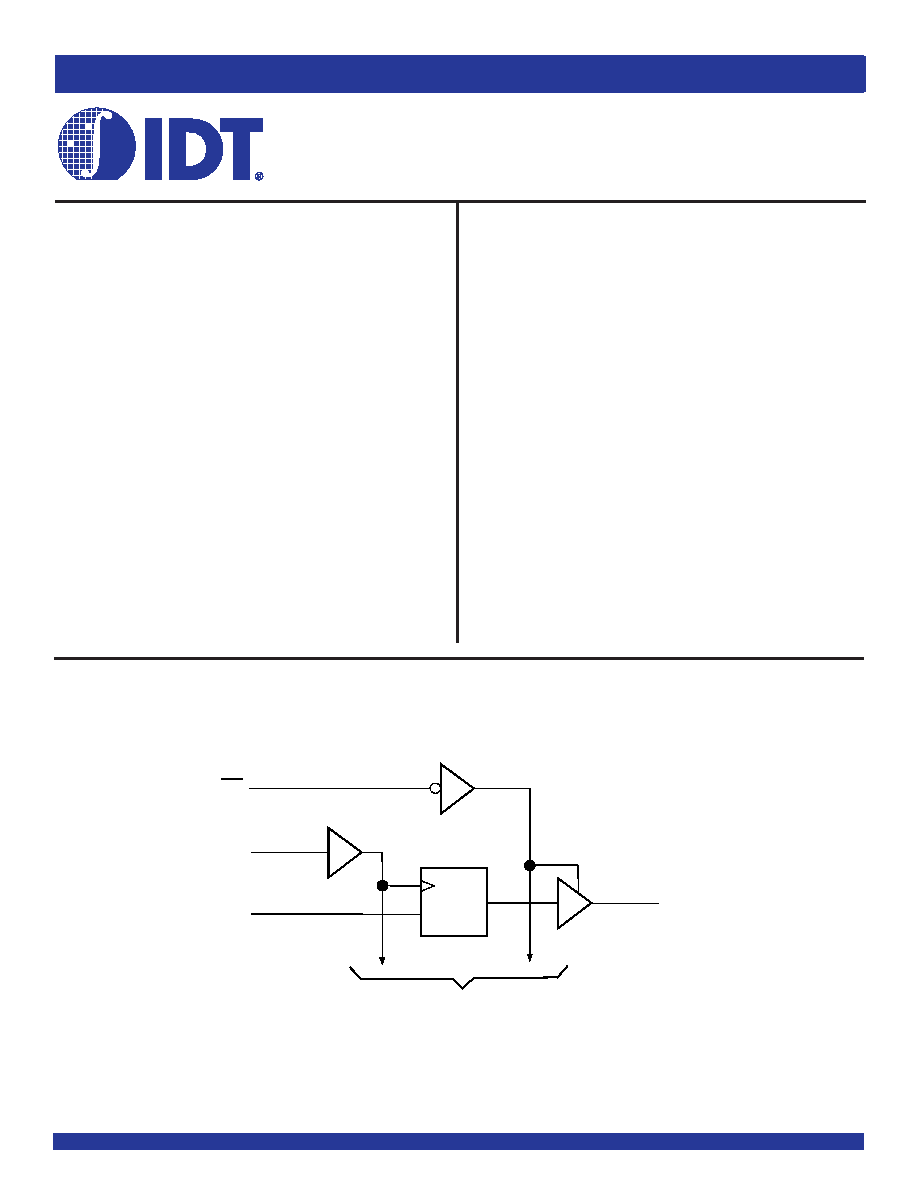
FUNCTIONAL BLOCK DIAGRAM
APPLICATIONS:
3.3V high speed systems
3.3V and lower voltage computing systems
DRIVE FEATURES:
High Output Drivers: ±24mA
Reduced system switching noise
IDT74LVCH574A
DESCRIPTION:
The LVCH574A octal edge-triggered D-type flip-flop is built using ad-
vanced dual-metal CMOS technology. The device features 3-state outputs
designed specifically for driving highly capacitive or relatively low-imped-
ance loads. The LVCH574A is particularly suitable for implementing buffer
registers, input-output (I/O) ports, bidirectional bus drivers, and working
registers.
On the positive transition of the clock (CLK) input, the Q outputs are set to
the logic levels at the data (D) inputs.
A buffered output-enable (OE) input can be used to place the eight outputs
in either a normal logic state (high or low logic levels) or a high-impedance
state. In the high- impedance state, the outputs neither load nor drive the bus
lines significantly. OEdoes not affect the internal operations of the flip-flops.
Old data can be retained or new data can be entered while the outputs are
in the high-impedance state.
The LVCH574A has been designed with a ±24mA output driver. This
driver is capable of driving a moderate to heavy load while maintaining speed
performance.
Inputs can be driven from either 3.3V or 5V devices. This feature allows
the use of this device as a translator in a mixed 3.3V/5V system environment.
The LVCH574A has “bus-hold” which retains the inputs’ last state
whenever the input goes to a high impedance. This prevents floating inputs
and eliminates the need for pull-up/down resistors.
3.3V CMOS OCTAL EDGE-
TRIGGERED D-TYPE FLIP-FLOP
WITH 3-STATE OUTPUTS, 5 VOLT
TOLERANT I/O AND BUS-HOLD
OE
C1
CLK
1
D
TO SEVEN OTHER CHANNELS
1
11
2
19
1
D
1
Q
相关PDF资料 |
PDF描述 |
|---|---|
| IDT74LVCH646APY | LVC/LCX/Z SERIES, 8-BIT REGISTERED TRANSCEIVER, TRUE OUTPUT, PDSO24 |
| IDT74LVCH646ASO8 | LVC/LCX/Z SERIES, 8-BIT REGISTERED TRANSCEIVER, TRUE OUTPUT, PDSO24 |
| IDT74LVCH646AQ8 | LVC/LCX/Z SERIES, 8-BIT REGISTERED TRANSCEIVER, TRUE OUTPUT, PDSO24 |
| IDT74LVCHR16952APV | LVC/LCX/Z SERIES, DUAL 8-BIT REGISTERED TRANSCEIVER, TRUE OUTPUT, PDSO56 |
| IDT74SSTV16857PAG8 | SSTV SERIES, POSITIVE EDGE TRIGGERED D FLIP-FLOP, TRUE OUTPUT, PDSO48 |
相关代理商/技术参数 |
参数描述 |
|---|---|
| IDT74LVCHR162245APA | 制造商:Integrated Device Technology Inc 功能描述: |
| IDT74LVCHR162245APAG | 功能描述:IC BUS TRSCVR 3-ST 16BIT 48TSSOP RoHS:是 类别:集成电路 (IC) >> 逻辑 - 缓冲器,驱动器,接收器,收发器 系列:74LVCHR 标准包装:47 系列:74LVX 逻辑类型:缓冲器/线路驱动器,非反相 元件数:4 每个元件的位元数:1 输出电流高,低:4mA,4mA 电源电压:2 V ~ 3.6 V 工作温度:-40°C ~ 85°C 安装类型:表面贴装 封装/外壳:14-SOIC(0.209",5.30mm 宽) 供应商设备封装:14-SOIC 包装:管件 |
| IDT74LVCHR162245APAG8 | 功能描述:IC BUS TRSCVR 3-ST 16BIT 48TSSOP RoHS:是 类别:集成电路 (IC) >> 逻辑 - 缓冲器,驱动器,接收器,收发器 系列:74LVCHR 产品培训模块:Logic Packages 标准包装:39 系列:74AVCH 逻辑类型:收发器,非反相 元件数:2 每个元件的位元数:8 输出电流高,低:12mA,12mA 电源电压:1.2 V ~ 3.6 V 工作温度:-40°C ~ 85°C 安装类型:表面贴装 封装/外壳:48-TFSOP(0.240",6.10mm 宽) 供应商设备封装:48-TSSOP 包装:管件 产品目录页面:831 (CN2011-ZH PDF) 其它名称:568-2585-574AVCH16245DGG,512935266779512 |
| IDT74LVCHR16646APAG | 功能描述:IC SERIAL RTC LP W/I2C 56-TSSOP RoHS:是 类别:未定义的类别 >> 其它 系列:* 标准包装:1 系列:* 其它名称:MS305720A |
| IDT74LVCHR16646APAG8 | 功能描述:IC SERIAL RTC LP W/I2C 56-TSSOP RoHS:是 类别:未定义的类别 >> 其它 系列:* 标准包装:1 系列:* 其它名称:MS305720A |
发布紧急采购,3分钟左右您将得到回复。