- 您现在的位置:买卖IC网 > PDF目录4581 > IDT77V500S25BC8 (IDT, Integrated Device Technology Inc)IC SW MEMORY 8X8 1.2BGPS 144-BGA PDF资料下载
参数资料
| 型号: | IDT77V500S25BC8 |
| 厂商: | IDT, Integrated Device Technology Inc |
| 文件页数: | 2/17页 |
| 文件大小: | 0K |
| 描述: | IC SW MEMORY 8X8 1.2BGPS 144-BGA |
| 标准包装: | 1,000 |
| 系列: | SwitchStar™ |
| 类型: | 集成式开关控制器 |
| 安装类型: | 表面贴装 |
| 封装/外壳: | 144-LBGA |
| 供应商设备封装: | 144-CABGA(13x13) |
| 包装: | 带卷 (TR) |
| 其它名称: | 77V500S25BC8 |
10 of 17
April 11, 2001
IDT77V500
Manager Commands
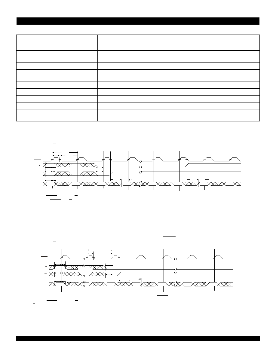
Manager Bus Read Timing Waveform
Write operations, both for Commands and Data, are synchronous to the rising edge of MSTRB. The data placed on the MDATA pins is determined
by the state of the MD/C pin.
1The combination of MSTRB Low and MR/W High (Read mode) asynchronously enables the MDATA pins as outputs. That is, data is available to be read one asynchronous tAMD time
after the falling edge of MSTRB if MR/W is High.
2After the Command is written, the Manager must take MR/W High (Read mode) to wait for a valid Command Acknowledge from the IDT77V500 before proceeding. Reading a High
Bit 7 of the status register under these conditions indicates the command has been acknowledged by the IDT77V500. This may take multiple IDT77V500 SCLK cycles based on possible
higher priority operations that the IDT77V500 must support.
3A valid Acknowledge from the IDT77V500 is indicated by a High Command Acknowledge bit (Bit 7 of the Status Register).
4Waveform illustrates first two bytes of data only. Additional bytes may be available based on command used.
Manager Bus Write Timing Waveform
Write operations, both for Commands and Data, are synchronous to the rising edge of MSTRB. The data placed on the MDATA pins is determined
by the state of the MD/C pin.
1Either a Read cycle was completed or a Status Acknowledge was executed immediately prior to the first MSTRB of this write waveform.
2The combination of MSTRB Low and MR/W High (Read mode) asynchronously enables the MDATA pins as outputs. The data placed on the MDATA pins is determined by the state
of the MD/C pin.
3After the Command is written, the Manager must take MR/W High (Read mode) to wait for a valid Command Acknowledge from the IDT77V500 before proceeding. Reading a High
Bit 7 of the status register under these conditions indicates the command has been acknowledged by the IDT77V500. This may take multiple IDT77V500 SCLK cycles based on possible
higher priority operations that the IDT77V500 must support.
4A valid Acknowledge from the IDT77V500 is indicated by a High Command Acknowledge bit (Bit 7 of the Status Register).
Command1
1. Manager Command codes not defined in this table are not to be used.
Command Name
Command Description
Code (in Hex)
WRSL
Write Service Link Memory
Write into Service Link Memory to initialize scheduled service lists.
03
STAT
Read IDT77V500 status
Reads the internal status of the IDT77V500. Available information includes various
error registers and counts.
07
LDCFG
Load IDT77V400 Configuration Bits Passes configuration information to the IDT77V400.
08
SUP
Call setup
Writes the appropriate information into an entry of the Per VC Memory to perform the
call setup function.
09
INT
Initialize IDT77V500
Initializes the internal configuration registers of the IDT77V500.
0A
SEL
Select a IDT77V500
Selects the IDT77V500 to be enabled in a multiple device configuration.
0B
START
End of IDT77V500 Initialization
Sets the IDT77V500 into an enabled state after it has been initialized.
0C
CBR
Set up a CBR Scheduler
Sets up a selected output service list in the Constant Bit Rate (CBR) mode.
0D
PARM
Set Parameters
Sets various parameters in the IDT77V500, including the CLP low water mark, the
EFCI low water mark, and the EPD low water mark.
0E
MD/C
MS TR B
MR/W
3607 drw 08
tSMRW
tHMRW
tSMD
tHMD
MDATA
tMCH
tMCL
tMCYC
tSM
tHM
Write first
8ADDRbits
Acknowledge Read
tAMD
DATAOUT
CMDIN
ADDRIN
tOHMD
Write last
8ADDRbits
Write Cycle-
Read Command
1
2
DATAOUT
3
Read Byte 0
Acknowledge Read
Acknowledge Read –
Valid Command Acknowledge
tAMD
tOHMD
tSMRW
tSM
Read Byte 1
4
MDATA
MS TR B
tSM
tHM
3607 drw 09
tSMRW tHMRW
tSMD
tHMD
MR/W
MD/C
tMCH
tMCL
tMCYC
DATAIN
CMDIN
DATAOUT
WriteDataByte0
Write Data Byte 12
Write Cycle-
Write Command
Acknowledge Read
tOHMD
T0
T12
tAMD
DATAOUT
2
3
Acknowledge Read
DATAOUT
4
Acknowledge Read
Acknowledge Read –
Valid Command Acknowledge
tSM
tSMRW
1
相关PDF资料 |
PDF描述 |
|---|---|
| LT1764AEFE-2.5#TRPBF | IC REG LDO 2.5V 3A 16TSSOP |
| LFXP10E-5F388C | IC FPGA 9.7KLUTS 244I/O 388-BGA |
| LFXP10E-4F388I | IC FPGA 9.7KLUTS 244I/O 388-BGA |
| LFXP10C-4F388I | IC FPGA 9.7KLUTS 244I/O 388-BGA |
| LFXP10E-4FN388I | IC FPGA 9.7KLUTS 388FPBGA |
相关代理商/技术参数 |
参数描述 |
|---|---|
| IDT77V500S25BCG | 功能描述:IC SW MEMORY 8X8 1.2BGPS 144-BGA RoHS:是 类别:集成电路 (IC) >> 专用 IC 系列:SwitchStar™ 产品培训模块:Lead (SnPb) Finish for COTS Obsolescence Mitigation Program 标准包装:1 系列:- 类型:调帧器 应用:数据传输 安装类型:表面贴装 封装/外壳:400-BBGA 供应商设备封装:400-PBGA(27x27) 包装:散装 |
| IDT77V500S25BCG8 | 功能描述:IC SW MEMORY 8X8 1.2BGPS 144-BGA RoHS:是 类别:集成电路 (IC) >> 专用 IC 系列:SwitchStar™ 产品培训模块:Lead (SnPb) Finish for COTS Obsolescence Mitigation Program 标准包装:1 系列:- 类型:调帧器 应用:数据传输 安装类型:表面贴装 封装/外壳:400-BBGA 供应商设备封装:400-PBGA(27x27) 包装:散装 |
| IDT77V500S25PF | 功能描述:IC SW MEMORY 8X8 1.2BGPS 100TQFP RoHS:否 类别:集成电路 (IC) >> 专用 IC 系列:SwitchStar™ 产品培训模块:Lead (SnPb) Finish for COTS Obsolescence Mitigation Program 标准包装:1 系列:- 类型:调帧器 应用:数据传输 安装类型:表面贴装 封装/外壳:400-BBGA 供应商设备封装:400-PBGA(27x27) 包装:散装 |
| IDT77V500S25PF8 | 功能描述:IC SW MEMORY 8X8 1.2BGPS 100TQFP RoHS:否 类别:集成电路 (IC) >> 专用 IC 系列:SwitchStar™ 产品培训模块:Lead (SnPb) Finish for COTS Obsolescence Mitigation Program 标准包装:1 系列:- 类型:调帧器 应用:数据传输 安装类型:表面贴装 封装/外壳:400-BBGA 供应商设备封装:400-PBGA(27x27) 包装:散装 |
| IDT77V550S25DT | 功能描述:IC SW MEMORY 8X8 1.2BGPS 80-TQFP RoHS:否 类别:集成电路 (IC) >> 专用 IC 系列:SwitchStar™ 产品培训模块:Lead (SnPb) Finish for COTS Obsolescence Mitigation Program 标准包装:1 系列:- 类型:调帧器 应用:数据传输 安装类型:表面贴装 封装/外壳:400-BBGA 供应商设备封装:400-PBGA(27x27) 包装:散装 |
发布紧急采购,3分钟左右您将得到回复。