- 您现在的位置:买卖IC网 > PDF目录1924 > IDT82V2088DRG (IDT, Integrated Device Technology Inc)IC LIU T1/J1/E1 8CH 208-TQFP PDF资料下载
参数资料
| 型号: | IDT82V2088DRG |
| 厂商: | IDT, Integrated Device Technology Inc |
| 文件页数: | 3/78页 |
| 文件大小: | 0K |
| 描述: | IC LIU T1/J1/E1 8CH 208-TQFP |
| 标准包装: | 12 |
| 类型: | 线路接口装置(LIU) |
| 规程: | E1 |
| 电源电压: | 3.13 V ~ 3.47 V |
| 安装类型: | 表面贴装 |
| 封装/外壳: | 208-BFQFP |
| 供应商设备封装: | 208-PQFP(28x28) |
| 包装: | 托盘 |
| 其它名称: | 82V2088DRG |
第1页第2页当前第3页第4页第5页第6页第7页第8页第9页第10页第11页第12页第13页第14页第15页第16页第17页第18页第19页第20页第21页第22页第23页第24页第25页第26页第27页第28页第29页第30页第31页第32页第33页第34页第35页第36页第37页第38页第39页第40页第41页第42页第43页第44页第45页第46页第47页第48页第49页第50页第51页第52页第53页第54页第55页第56页第57页第58页第59页第60页第61页第62页第63页第64页第65页第66页第67页第68页第69页第70页第71页第72页第73页第74页第75页第76页第77页第78页
11
INDUSTRIAL
TEMPERATURE RANGES
OCTAL CHANNEL T1/E1/J1 LONG HAUL/SHORT HAUL LINE INTERFACE UNIT
Transmit and Receive Digital Data Interface
TD1/TDP1
TD2/TDP2
TD3/TDP3
TD4/TDP4
TD5/TDP5
TD6/TDP6
TD7/TDP7
TD8/TDP8
TDN1
TDN2
TDN3
TDN4
TDN5
TDN6
TDN7
TDN8
Input
155
149
143
137
127
121
115
109
154
148
142
136
126
120
114
108
B15
D15
E15
G15
J15
L15
N15
R16
C14
D14
F13
G14
J14
L14
M13
P15
TDn: Transmit Data for Channel 1~8
In Single Rail Mode, the NRZ data to be transmitted is input on these pins. Data on TDn is sampled
into the device on the active edge of TCLKn. The active edge of TCLKn is selected by the TCLK_SEL
bit (TCF0, 02H...). Data is encoded by AMI, HDB3 or B8ZS line code rules before being transmitted to
the line. In this mode, TDNn should be connected to ground.
TDPn/TDNn: Positive/Negative Transmit Data for Channel 1~8
In Dual Rail Mode, the NRZ data to be transmitted is input on these pins. Data on TDPn/TDNn is sam-
pled into the device on the active edge of TCLKn. The active edge of the TCLKn is selected by the
TCLK_SEL bit (TCF0, 02H...) The line code in Dual Rail Mode is as follows:
TCLK1
TCLK2
TCLK3
TCLK4
TCLK5
TCLK6
TCLK7
TCLK8
Input
156
150
144
138
129
122
116
110
A15
C16
E16
G16
J16
L16
N16
T16
TCLKn: Transmit Clock for Channel 1~8
These pins input 1.544 MHz for T1/J1 mode or 2.048 MHz for E1 mode transmit clock. The transmit
data on TDn/TDPn or TDNn is sampled into the device on the active edge of TCLKn. If TCLKn is
missing1 and the TCLKn missing interrupt is not masked, an interrupt will be generated.
RD1/RDP1
RD2/RDP2
RD3/RDP3
RD4/RDP4
RD5/RDP5
RD6/RDP6
RD7/RDP7
RD8/RDP8
CV1/RDN1
CV2/RDN2
CV3/RDN3
CV4/RDN4
CV5/RDN5
CV6/RDN6
CV7/RDN7
CV8/RDN8
Output
152
146
140
134
124
118
112
106
151
145
139
132
123
117
111
105
B16
E14
F15
H14
K14
M15
N14
P14
C15
E13
F14
H13
K13
M14
N13
R15
RDn: Receive Data for Channel 1~8
In Single Rail Mode, the NRZ receive data is output on these pins. Data is decoded according to AMI,
HDB3 or B8ZS line code rules. The active level on RDn pin is selected by the RD_INV bit (RCF0,
07H...).
CVn: Code Violation for Channel 1~8
In Single Rail Mode, the BPV/CV errors in received data streams will be reported by driving pin CVn
to high level for a full clock cycle. The B8ZS/HDB3 line code violation can be indicated when the B8ZS/
HDB3 decoder is enabled. When AMI decoder is selected, the bipolar violation can be indicated.
RDPn/RDNn: Positive/Negative Receive Data for Channel 1~8
In Dual Rail Mode with Clock & Data Recovery (CDR), these pins output the NRZ data with the recov-
ered clock. An active level on RDPn indicates the receipt of a positive pulse on RTIPn/RRINGn while
an active level on RDNn indicates the receipt of a negative pulse on RTIPn/RRINGn. The active level
on RDPn/RDNn is selected by the RD_INV bit (RCF0, 07H...). When CDR is disabled, these pins
directly output the raw RZ sliced data. The output data on RDn and RDPn/RDNn is updated on the
active edge of RCLKn.
RCLK1
RCLK2
RCLK3
RCLK4
RCLK5
RCLK6
RCLK7
RCLK8
Output
153
147
141
135
125
119
113
107
A16
D16
F16
H15
K15
M16
P16
T15
RCLKn: Receive Clock for Channel 1~8
These pins output 1.544 MHz for T1/J1 mode or 2.048 MHz for E1 mode receive clock. Under LOS
conditions, if AISE bit (MAINT0, 0AH...) is ‘1’, RCLKn is derived from MCLK.
In clock recovery mode, these pins provide the clock recovered from the signal received on RTIPn/
RRINGn. The receive data (RDn in Single Rail Mode or RDPn/RDNn in Dual Rail Mode) is updated on
the active edge of RCLKn. The active edge is selected by the RCLK_SEL bit (RCF0, 07H...).
If clock recovery is bypassed, RCLKn is the exclusive OR(XOR) output of the Dual Rail sliced data
RDPn and RDNn. This signal can be used in the applications with external clock recovery circuitry.
Table-1 Pin Description (Continued)
Name
Type
Pin No.
Description
PQFP208
PBGA208
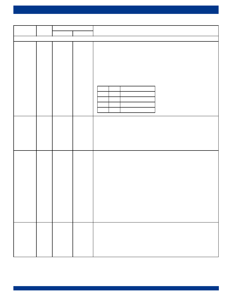
TDPn
TDNn
Output Pulse
0
Space
0
1
Positive Pulse
1
0
Negative Pulse
1
Space
Notes:
1. TCLKn missing: the state of TCLKn continues to be high level or low level over 70 clock cycles.
相关PDF资料 |
PDF描述 |
|---|---|
| IDT82V2108BBG | IC FRAMER T1/J1/E1 8CH 144-BGA |
| IDT82V2604BBG | IC INVERSE MUX 4CH ATM 208-BGA |
| IDT82V2608BBG | IC INVERSE MUX 8CH ATM 208-BGA |
| IDT82V2616BBG | IC INVERSE MUX 16CH ATM 272-PBGA |
| IDT88K8483BRI | IC SPI-4 EXCHANGE 3PORT 672-BGA |
相关代理商/技术参数 |
参数描述 |
|---|---|
| IDT82V2108 | 制造商:IDT 制造商全称:Integrated Device Technology 功能描述:T1 / E1 / J1 OCTAL FRAMER |
| IDT82V2108BB | 功能描述:IC FRAMER T1/J1/E1 8CH 144-BGA RoHS:否 类别:集成电路 (IC) >> 接口 - 控制器 系列:- 标准包装:4,900 系列:- 控制器类型:USB 2.0 控制器 接口:串行 电源电压:3 V ~ 3.6 V 电流 - 电源:135mA 工作温度:0°C ~ 70°C 安装类型:表面贴装 封装/外壳:36-VFQFN 裸露焊盘 供应商设备封装:36-QFN(6x6) 包装:* 其它名称:Q6396337A |
| IDT82V2108BBG | 功能描述:IC FRAMER T1/J1/E1 8CH 144-BGA RoHS:是 类别:集成电路 (IC) >> 接口 - 控制器 系列:- 标准包装:4,900 系列:- 控制器类型:USB 2.0 控制器 接口:串行 电源电压:3 V ~ 3.6 V 电流 - 电源:135mA 工作温度:0°C ~ 70°C 安装类型:表面贴装 封装/外壳:36-VFQFN 裸露焊盘 供应商设备封装:36-QFN(6x6) 包装:* 其它名称:Q6396337A |
| IDT82V2108PX | 功能描述:IC FRAMER T1/J1/E1 8CH 128-PQFP RoHS:否 类别:集成电路 (IC) >> 接口 - 控制器 系列:- 标准包装:4,900 系列:- 控制器类型:USB 2.0 控制器 接口:串行 电源电压:3 V ~ 3.6 V 电流 - 电源:135mA 工作温度:0°C ~ 70°C 安装类型:表面贴装 封装/外壳:36-VFQFN 裸露焊盘 供应商设备封装:36-QFN(6x6) 包装:* 其它名称:Q6396337A |
| IDT82V2108PX8 | 功能描述:IC FRAMER T1/J1/E1 8CH 128-PQFP RoHS:否 类别:集成电路 (IC) >> 接口 - 控制器 系列:- 标准包装:4,900 系列:- 控制器类型:USB 2.0 控制器 接口:串行 电源电压:3 V ~ 3.6 V 电流 - 电源:135mA 工作温度:0°C ~ 70°C 安装类型:表面贴装 封装/外壳:36-VFQFN 裸露焊盘 供应商设备封装:36-QFN(6x6) 包装:* 其它名称:Q6396337A |
发布紧急采购,3分钟左右您将得到回复。