- 您现在的位置:买卖IC网 > PDF目录377488 > IDT82V3010PVG (INTEGRATED DEVICE TECHNOLOGY INC) T1/E1/OC3 TELECOM CLOCK GENERATOR WITH DUAL REFERENCE INPUTS PDF资料下载
参数资料
| 型号: | IDT82V3010PVG |
| 厂商: | INTEGRATED DEVICE TECHNOLOGY INC |
| 元件分类: | 通信及网络 |
| 英文描述: | T1/E1/OC3 TELECOM CLOCK GENERATOR WITH DUAL REFERENCE INPUTS |
| 中文描述: | SPECIALTY TELECOM CIRCUIT, PDSO56 |
| 封装: | GREEN, SSOP-56 |
| 文件页数: | 11/31页 |
| 文件大小: | 355K |
| 代理商: | IDT82V3010PVG |
第1页第2页第3页第4页第5页第6页第7页第8页第9页第10页当前第11页第12页第13页第14页第15页第16页第17页第18页第19页第20页第21页第22页第23页第24页第25页第26页第27页第28页第29页第30页第31页
IDT82V3010
T1/E1/OC3 Telecom Clock Generator with Dual Reference Inputs
Functional Description
11
June 19, 2006
Reference Input Monitor and Invalid Input Signal Detection block for
further processing.
When a transient voltage occurs on the IN_sel pin, the operating
mode will be changed to Short Time Holdover (S4) with the TIE Control
Block automatically disabled. At the stage of S4, if no IN_sel transient
occurs, the reference signal will be switched from one to the other, and
the operating mode will be changed back to Normal (S1) automatically.
During the change from S4 to S1, the TIE Control Block can be enabled
or disabled, depending on the logic level on the TIE_en pin. See
Figure -
3
for details.
2.4
REFERENCE INPUT MONITOR
The IDT82V3010 monitors the Fref0 and Fref1 frequencies and
outputs two signals at MON_out0 pin and MON_out1 pin to indicate the
monitoring results respectively. Whenever the Fref0 frequency is off the
nominal frequency by more than ±12 ppm, the MON_out0 pin will go
high. The MON_out1 pin indicates the monitoring result of Fref1 in the
same way. The MON_out0 and MON_out1 signals are updated every 2
seconds.
2.5
INVALID INPUT SIGNAL DETECTION
This circuit is used to detect if the selected input reference (Fref0 or
Fref1) is out of the capture range. Refer to
“3.6 Capture Range”
for
details. This includes a complete loss of the input reference and a large
frequency shift in the input reference.
If the input reference is invalid (out of the capture range), the
IDT82V3010 will be automatically changed to the Holdover mode (Auto-
Holdover). When the input reference becomes valid, the device will be
changed back to the Normal mode and the output signals will be locked
to the input reference.
In the Holdover mode, the output signals are based on the output
reference signal 30 ms to 60 ms prior to entering the Holdover mode.
The amount of phase drift while in holdover can be negligible because
the Holdover mode is very accurate. Consequently, the phase delay
between the input and output after switching back to the Normal mode is
preserved.
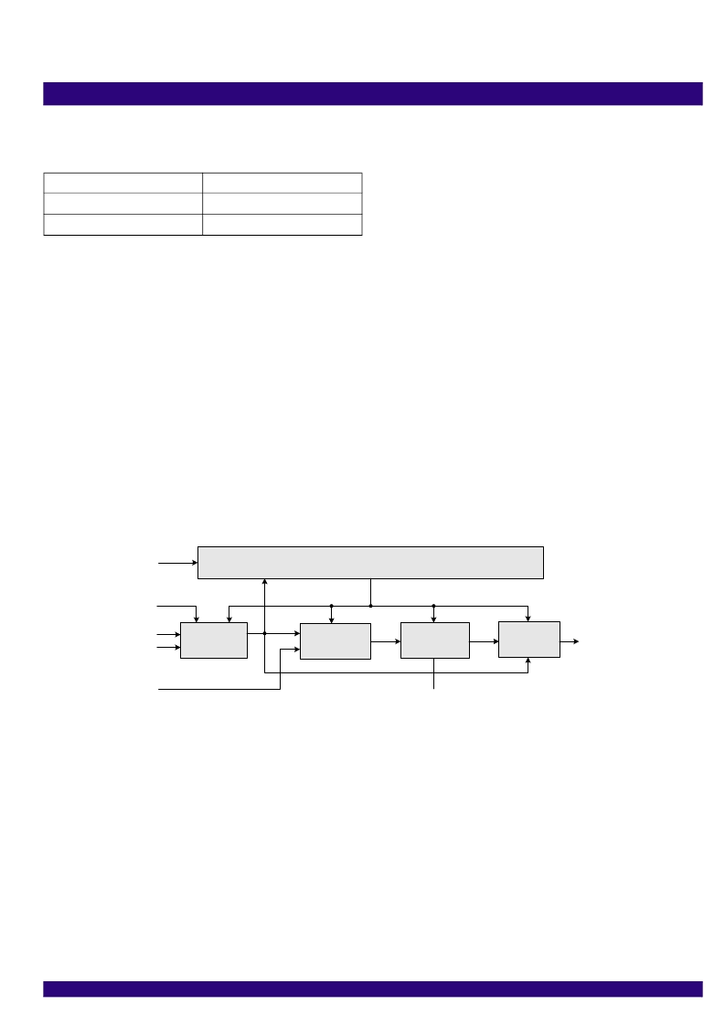
2.6
TIE CONTROL BLOCK
If the current reference is badly damaged or lost, it is necessary to
use the other reference or the one generated by storage techniques
instead. But when switching the reference, a step change in phase on
the input reference will occur. A step change in phase in the input to
DPLL may lead to an unacceptable phase change on the output signals.
The TIE control block, when enabled, prevents a step change in phase
on the input reference signals from causing a step change in phase on
the output of the DPLL block.
Figure - 4
shows the TIE Control Block
diagram.
Figure - 4 TIE Control Block Diagram
When the TIE Control Block is enabled manually or automatically (by
the TIE_en pin or TIE auto-enable logic generated by the State Control
Circuit), it works under the control of the Step Generation circuit.
At the Measure Circuit stage, the selected reference signal (Fref0 or
Fref1) is compared with the feedback signal (current output feed back
from the Frequency Select Circuit). The phase difference between the
input reference and the feedback signal is stored in the Storage Circuit
for TIE correction. According to the value stored in the storage circuit,
the Trigger Circuit generates a virtual reference with the same phase as
the previous reference. In this way, the reference can be switched
without generating a step change in phase.
Figure - 5
shows the phase transient that will result if a reference
switch is performed with the TIE Control Block enabled.
The value of the phase difference in the Storage Circuit can be
cleared by applying a logic low reset signal to the
TCLR
pin. The
minimum width of the reset pulse should be 300 ns.
When the IDT82V3010 primarily enters the Holdover mode for a
short time period and then returns back to the Normal mode, the TIE
Control Circuit should not be enabled. This will prevent undesired
accumulated phase change between the input and output.
If the TIE Control Block is disabled manually or automatically, a
reference switch will result in a phase alignment between the input
signal and the output signal as shown in
Figure - 6
. The slope of the
phase adjustment is limited to 5 ns per 125 μs.
Table - 4 Input Reference Selection
IN_sel
Input Reference
0
Fref0
1
Fref1
Step Generation
TIE_en
Reference
Select Circuit
Fref0
Fref1
IN_sel
Measure
Circuit
Storage
Circuit
Trigger
Circuit
Feedback
Signal
TCLR
Fref
Virtual
Reference
Signal
相关PDF资料 |
PDF描述 |
|---|---|
| IDT82V3255 | WAN PLL |
| IDT82V3255DK | WAN PLL |
| IDT82V3255DKG | WAN PLL |
| IDT82V3255TF | WAN PLL |
| IDT82V3255TFG | WAN PLL |
相关代理商/技术参数 |
参数描述 |
|---|---|
| IDT82V3010PVG8 | 功能描述:IC PLL WAN 51/E1/OC3 DUAL 56SSOP RoHS:是 类别:集成电路 (IC) >> 时钟/计时 - 专用 系列:- 标准包装:1,500 系列:- 类型:时钟缓冲器/驱动器 PLL:是 主要目的:- 输入:- 输出:- 电路数:- 比率 - 输入:输出:- 差分 - 输入:输出:- 频率 - 最大:- 电源电压:3.3V 工作温度:0°C ~ 70°C 安装类型:表面贴装 封装/外壳:28-SSOP(0.209",5.30mm 宽) 供应商设备封装:28-SSOP 包装:带卷 (TR) 其它名称:93786AFT |
| IDT82V3011 | 制造商:IDT 制造商全称:Integrated Device Technology 功能描述:T1/E1/OC3 WAN PLL WITH SINGLE REFERENCE INPUT |
| IDT82V3011PV | 制造商:INT_DEV_TECH 功能描述: |
| IDT82V3011PVG | 功能描述:IC PLL WAN T1/E1/OC3 SGL 56-SSOP RoHS:是 类别:集成电路 (IC) >> 时钟/计时 - 专用 系列:- 标准包装:1,500 系列:- 类型:时钟缓冲器/驱动器 PLL:是 主要目的:- 输入:- 输出:- 电路数:- 比率 - 输入:输出:- 差分 - 输入:输出:- 频率 - 最大:- 电源电压:3.3V 工作温度:0°C ~ 70°C 安装类型:表面贴装 封装/外壳:28-SSOP(0.209",5.30mm 宽) 供应商设备封装:28-SSOP 包装:带卷 (TR) 其它名称:93786AFT |
| IDT82V3011PVG8 | 功能描述:IC PLL WAN T1/E1/OC3 SGL 56-SSOP RoHS:是 类别:集成电路 (IC) >> 时钟/计时 - 专用 系列:- 标准包装:1,500 系列:- 类型:时钟缓冲器/驱动器 PLL:是 主要目的:- 输入:- 输出:- 电路数:- 比率 - 输入:输出:- 差分 - 输入:输出:- 频率 - 最大:- 电源电压:3.3V 工作温度:0°C ~ 70°C 安装类型:表面贴装 封装/外壳:28-SSOP(0.209",5.30mm 宽) 供应商设备封装:28-SSOP 包装:带卷 (TR) 其它名称:93786AFT |
发布紧急采购,3分钟左右您将得到回复。