- 您现在的位置:买卖IC网 > PDF目录65593 > IDTCSP59910-5SO (INTEGRATED DEVICE TECHNOLOGY INC) PLL BASED CLOCK DRIVER, 8 TRUE OUTPUT(S), 0 INVERTED OUTPUT(S), PDSO24 PDF资料下载
参数资料
| 型号: | IDTCSP59910-5SO |
| 厂商: | INTEGRATED DEVICE TECHNOLOGY INC |
| 元件分类: | 时钟及定时 |
| 英文描述: | PLL BASED CLOCK DRIVER, 8 TRUE OUTPUT(S), 0 INVERTED OUTPUT(S), PDSO24 |
| 封装: | 0.300 INCH, SOIC-24 |
| 文件页数: | 1/6页 |
| 文件大小: | 96K |
| 代理商: | IDTCSP59910-5SO |
1
COMMERCIALANDINDUSTRIALTEMPERATURERANGES
IDTCSP59910
LOW SKEW PLL CLOCK DRIVER TURBOCLOCK JR.
G ND/sO E
Q0
Q1
REF
FS
PLL
FB
VCCQ/PE
Q2
Q3
Q4
Q5
Q6
Q7
FEBRUARY 2000
2000
Integrated Device Technology, Inc.
DSC-5812/-
c
IDTCSP59910
COMMERCIAL/INDUSTRIAL TEMPERATURE RANGES
LOW SKEW
PLL CLOCK DRIVER
TURBOCLOCK JR.
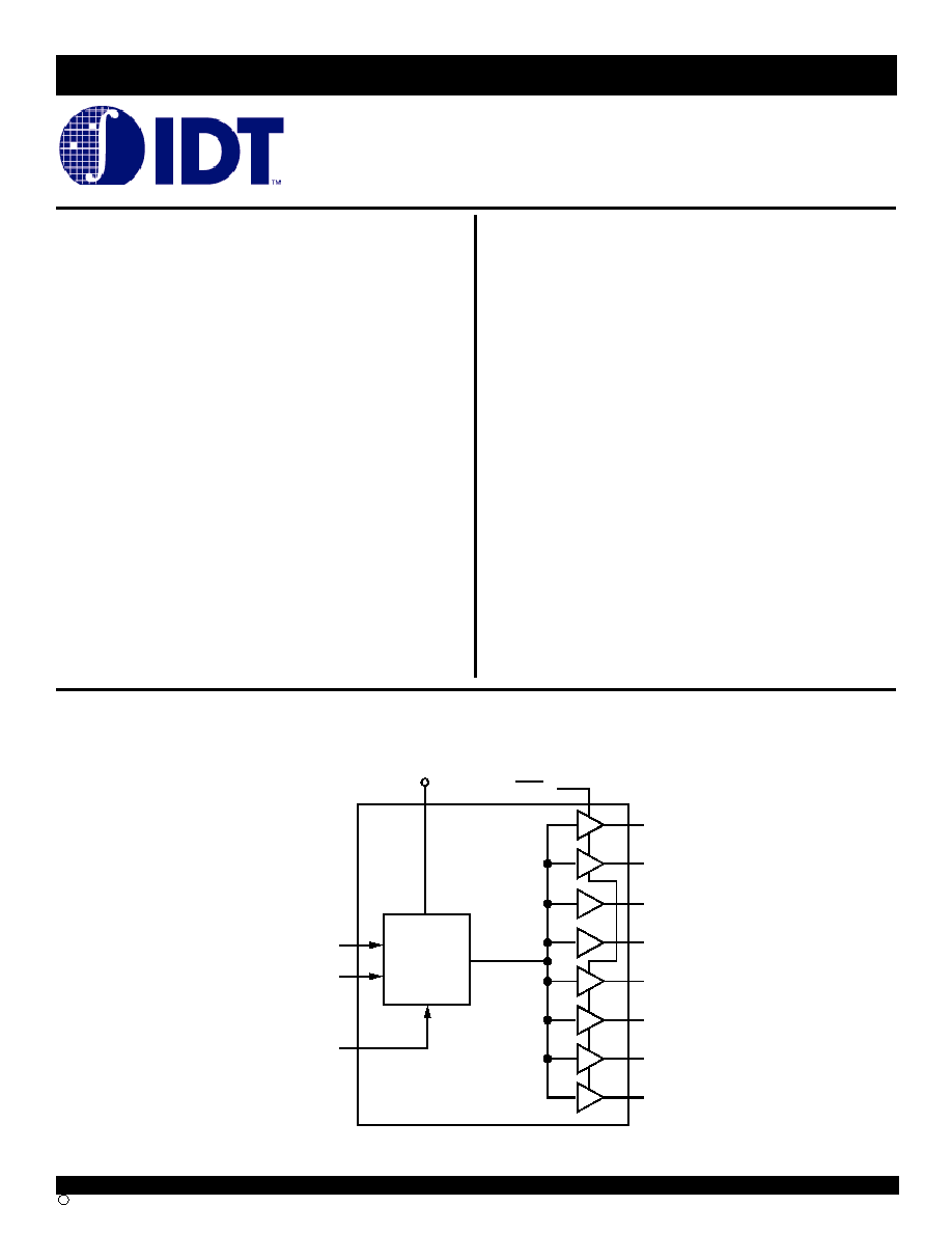
DESCRIPTION:
The CSP59910 is a high fanout phase lock loop clock driver in-
tended for high performance computing and data-communications ap-
plications. The CSP59910 has eight zero delay TTL outputs.
The CSP59910 maintains Cypress CY7B9910 compatibility while
providing two additional features: Synchronous Output Enable (GND/
sOE), and Positive/Negative Edge Synchronization (VCCQ/PE). When
the GND/
sOE pin is held low, all the outputs are synchronously en-
abled (CY7B9910 compatibility). However, if GND/
sOE is held high, all
the outputs except Q2 and Q3 are synchronously disabled.
Furthermore, when the VCCQ/PE is held high, all the outputs are
synchronized with the positive edge of the REF clock input (CY7B9910
compatibility). When VCCQ/PE is held low, all the outputs are synchro-
nized with the negative edge of REF.
The FB signal is compared with the input REF signal at the phase
detector in order to drive the VCO. Phase differences cause the VCO
of the PLL to adjust upwards or downwards accordingly.
An internal loop filter moderates the response of the VCO to the
phase detector. The loop filter transfer function has been chosen to
provide minimal jitter (or frequency variation) while still providing accu-
rate responses to input frequency changes.
FEATURES:
Eight zero delay outputs
Selectable positive or negative edge synchronization
Synchronous output enable
Output frequency: 25MHz to 85MHz
TTL outputs
3 skew grades:
CSP59910-2: t
SKEW0 <250ps
CSP59910-5: t
SKEW0 <500ps
CSP59910-7: t
SKEW0 <750ps
3-level input for PLL range control
PLL bypass for DC testing
External feedback, internal loop filter
46mA I
OL high drive outputs
Low Jitter: <200ps peak-to-peak
Outputs drive 50
terminatedlines
Pin compatible with Cypress CY7B9910
Available in SOIC Package
FUNCTIONAL BLOCK DIAGRAM
相关PDF资料 |
PDF描述 |
|---|---|
| IDTCSP59910-7SO | PLL BASED CLOCK DRIVER, 8 TRUE OUTPUT(S), 0 INVERTED OUTPUT(S), PDSO24 |
| IDTCSP5992-2JR | PLL BASED CLOCK DRIVER, 8 TRUE OUTPUT(S), 0 INVERTED OUTPUT(S), PQCC32 |
| IDTCSP5992-5JRI | PLL BASED CLOCK DRIVER, 8 TRUE OUTPUT(S), 0 INVERTED OUTPUT(S), PQCC32 |
| IDTCSP5V991-5JR | PLL BASED CLOCK DRIVER, 8 TRUE OUTPUT(S), 0 INVERTED OUTPUT(S), PQCC32 |
| IDTCSP5V991-2JR | PLL BASED CLOCK DRIVER, 8 TRUE OUTPUT(S), 0 INVERTED OUTPUT(S), PQCC32 |
相关代理商/技术参数 |
参数描述 |
|---|---|
| IDTCSPF2510C | 制造商:IDT 制造商全称:Integrated Device Technology 功能描述:3.3V PHASE-LOCK LOOP CLOCK DRIVER |
| IDTCSPF2510CPG | 制造商:IDT 制造商全称:Integrated Device Technology 功能描述:3.3V PHASE-LOCK LOOP CLOCK DRIVER |
| IDTCSPF2510CPGG | 制造商:IDT 制造商全称:Integrated Device Technology 功能描述:3.3V PHASE-LOCK LOOP CLOCK DRIVER |
| IDTCSPF2510CPGGI | 制造商:IDT 制造商全称:Integrated Device Technology 功能描述:3.3V PHASE-LOCK LOOP CLOCK DRIVER |
| IDTCSPF2510CPGI | 制造商:IDT 制造商全称:Integrated Device Technology 功能描述:3.3V PHASE-LOCK LOOP CLOCK DRIVER |
发布紧急采购,3分钟左右您将得到回复。