- 您现在的位置:买卖IC网 > PDF目录61093 > IL213A (VISHAY INTERTECHNOLOGY INC) 1 CHANNEL TRANSISTOR OUTPUT OPTOCOUPLER PDF资料下载
参数资料
| 型号: | IL213A |
| 厂商: | VISHAY INTERTECHNOLOGY INC |
| 元件分类: | 光电耦合器 |
| 英文描述: | 1 CHANNEL TRANSISTOR OUTPUT OPTOCOUPLER |
| 封装: | SOIC-8 |
| 文件页数: | 1/3页 |
| 文件大小: | 377K |
| 代理商: | IL213A |
Document Number: 83615
www.vishay.com
Revision 17-August-01
2–111
IL211AT/212AT/213AT
Phototransistor
Small Outline Surface Mount
Optocoupler
FEATURES
High Current Transfer Ratio
IL211A, 20% Minimum
IL212A, 50% Minimum
IL213A, 100% Minimum
Isolation Voltage, 3000 VRMS
Electrical Specications Similar to
Standard 6 Pin Coupler
Industry Standard SOIC-8A Surface
Mountable Package
Standard Lead Spacing, .05"
Available only on Tape and Reel Option
(Conforms to EIA Standard RS481A)
Compatible with Dual Wave, Vapor Phase
and IR Reow Soldering
Underwriters Lab File #E52744
(Code Letter Y)
VDE 0884 Available with Option 1
DESCRIPTION
The IL211AT/212AT/213AT are optically coupled pairs
with a Gallium Arsenide infrared LED and a silicon
NPN phototransistor. Signal information, including a
DC level, can be transmitted by the device while main-
taining a high degree of electrical isolation between
input and output. The IL211AT/212AT/213AT comes in
a standard SOIC-8 small outline package for surface
mounting which makes it ideally suited for high density
applications with limited space. In addition to eliminat-
ing through-holes requirements, this package con-
forms to standards for surface mounted devices.
A choice of 20, 50, and 100% minimum CTR at
IF=10 mA makes these optocouplers suitable for
a variety of different applications.
Maximum Ratings
Emitter
Peak Reverse Voltage .................................. 6.0 V
Continuous Forward Current ...................... 60 mA
Power Dissipation at 25
°C......................... 90 mW
Derate Linearly from 25
°C................... 1.2 mW/°C
Detector
Collector-Emitter Breakdown Voltage............ 30 V
Emitter-Collector Breakdown Voltage........... 7.0 V
Collector-Base Breakdown Voltage............... 70 V
ICMAX DC ..................................................... 50 mA
ICMAX (t<1.0 ms)....................................... 100 mA
Power Dissipation ................................... 150 mW
Derate Linearly from 25
°C................... 2.0 mW/°C
Package
Total Package Dissipation at 25
°C Ambient
(LED + Detector).................................. 240 mW
Derate Linearly from 25
°C................... 3.2 mW/°C
Storage Temperature ................ –55
°C to +150°C
Operating Temperature ............ –55
°C to +100°C
Soldering Time at 260
°C ...........................10 sec.
V
DE
Characteristics TA=25°C
Parameter
Symbol
Min.
Typ.
Max.
Unit
Condition
Emitter
Forward Voltage
VF
—
1.3
1.5
V
IF=10 mA
Reverse Current
IR
—
0.1
100
A
VR=6.0 V
Capacitance
C0
—13
—
pF
VR=0
Detector
Breakdown Voltage
BVCEO
30
——V
IC=10 A
BVECO
7.0
—
V
IE=10 A
Dark Current,
Collector-Emitter
ICEOdark —
5.0
50
nA
VCE=10 V
IF=0
Capacitance,
Collector-Emitter
CCE
—10
—
pF
VCE=0
Package
DC
Current
Transfer
Ratio
IL211AT
CTRDC
20
50
—
%
IF=10 mA,
VCE=5.0 V
IL212AT
50
80
—
IL213AT
100
130
—
Saturation Voltage,
Collector-Emitter
VCEsat
—
0.4
—
IF=10 mA,
IC=2.0 mA
Isolation Test
Voltage
VIO
3000
—
VRMS
1 sec.
Capacitance,
Input to Output
CIO
—
0.5
—
pF
—
Resistance,
Input to Output
RIO
—
100
—
G
—
Switching Time
ton, toff
—
3.0
—
s
IC=2.0 mA,
RL=100 ,
VCC=10 V
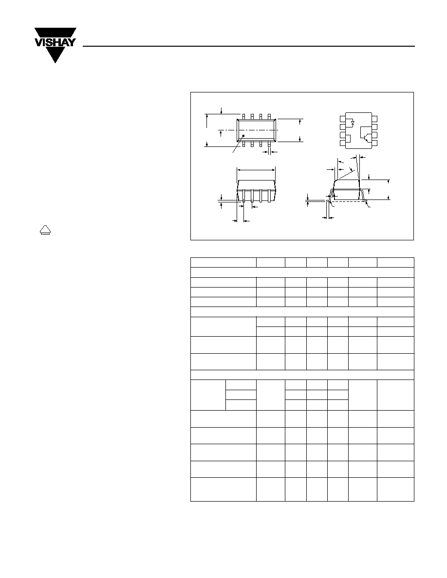
40
°
.240
(6.10)
.154
±.005
(3.91
±.13)
.050 (1.27)
typ.
.016 (.41)
.192
±.005
(4.88
±.13)
.004 (.10)
.008 (.20)
Lead
Coplanarity
±.0015 (.04)
max.
.015
±.002
(.38
±.05)
.008 (.20)
7
°
.058
±.005
(1.49
±.13)
.125
±.005
(3.18
±.13)
Pin One ID
.120
±.005
(3.05
±.13)
CL
.021 (.53)
5
° max.
R.010
(.25) max.
.020
±.004
(.51
±.10)
2 plcs.
1
2
3
4
Anode
Cathode
NC
8
7
6
5
NC
Base
Collector
Emitter
Dimensions in inches (mm)
相关PDF资料 |
PDF描述 |
|---|---|
| IL215AT-1 | 1 CHANNEL TRANSISTOR OUTPUT OPTOCOUPLER |
| IL216AT-1 | 1 CHANNEL TRANSISTOR OUTPUT OPTOCOUPLER |
| IL215AT | 1 CHANNEL TRANSISTOR OUTPUT OPTOCOUPLER |
| IL215AT | 1 CHANNEL TRANSISTOR OUTPUT OPTOCOUPLER |
| IL217AT | 1 CHANNEL TRANSISTOR OUTPUT OPTOCOUPLER |
相关代理商/技术参数 |
参数描述 |
|---|---|
| IL213A | 制造商:Vishay Intertechnologies 功能描述:OPTOCOUPLER SMD TRANSISTOR O/P |
| IL213AT | 功能描述:晶体管输出光电耦合器 Phototransistor Out Single CTR >100% RoHS:否 制造商:Vishay Semiconductors 输入类型:DC 最大集电极/发射极电压:70 V 最大集电极/发射极饱和电压:0.4 V 绝缘电压:5300 Vrms 电流传递比:100 % to 200 % 最大正向二极管电压:1.65 V 最大输入二极管电流:60 mA 最大集电极电流:100 mA 最大功率耗散:100 mW 最大工作温度:+ 110 C 最小工作温度:- 55 C 封装 / 箱体:DIP-4 封装:Bulk |
| IL213T | 制造商:未知厂家 制造商全称:未知厂家 功能描述:Optoelectronic |
| IL215 | 制造商:未知厂家 制造商全称:未知厂家 功能描述:SMALL OUTLINE OPTICALLY COUPLED ISOLATOR TRANSISTOR OUTPUT |
| IL215A | 制造商:INFINEON 制造商全称:Infineon Technologies AG 功能描述:PHOTOTRANSISTOR SMALL OUTLINE SURFACE MOUNT OPTOCOUPLER |
发布紧急采购,3分钟左右您将得到回复。