- 您现在的位置:买卖IC网 > PDF目录67720 > IMIC9806AYB PROC SPECIFIC CLOCK GENERATOR, PDSO48 PDF资料下载
参数资料
| 型号: | IMIC9806AYB |
| 元件分类: | 时钟产生/分配 |
| 英文描述: | PROC SPECIFIC CLOCK GENERATOR, PDSO48 |
| 封装: | SSOP-48 |
| 文件页数: | 10/15页 |
| 文件大小: | 178K |
| 代理商: | IMIC9806AYB |
C9806
I
2C Frequency Clock Generator for Mobil Pentium II Applications.
Approved Product
INTERNATIONAL MICROCIRCUITS, INC. 525 LOS COCHES ST.
Rev.1.4
9/2/1999
MILPITAS, CA 95035. TEL: 408-263-6300. FAX 408-263-6571
Page 4 of 15
http://www.imicorp.com
2-Wire I
2C Control Interface
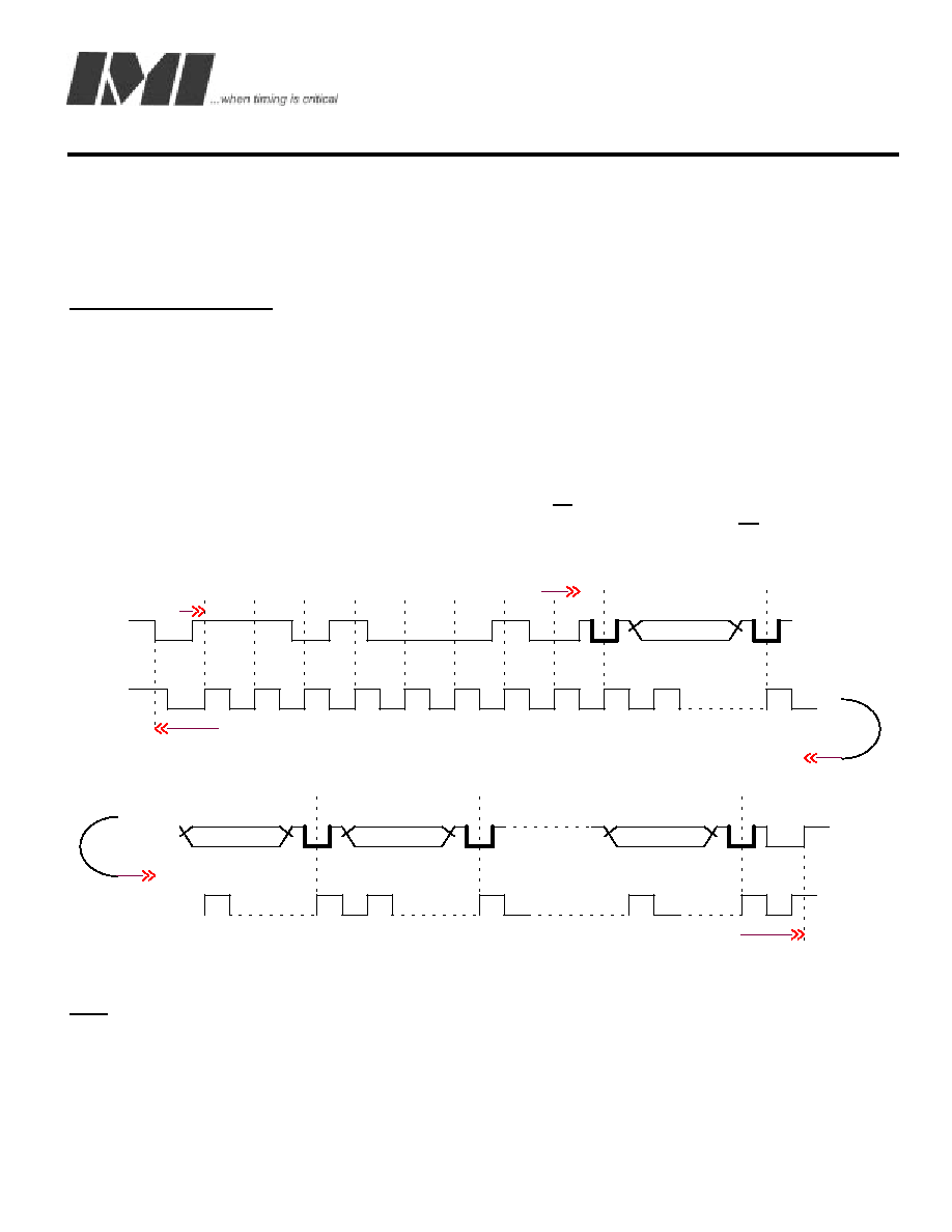
The 2-wire control interface implements a read/write slave only interface according to Philips I2C specification. (See
fig3). The device can be read back by using standard I
2C command bytes. Sub addressing is not supported, thus all
preceding bytes must be sent in order to change one of the control bytes. The 2-wire control interface allows each clock
output to be individually enabled or disabled. 100 Kbits/second (standard mode) data transfer is supported. It also allows
24/48 MHz frequency selection and test mode enable as well as Spread Spectrum programmability.
During normal data transfer, the SDATA signal only changes when the SCLK signal is low, and is stable when SCLK is
high. There are two exceptions to this. A high to low transition on SDATA while SCLK is high is used to indicate the
start of a data transfer cycle. A low to high transition on SDATA while SCLK is high indicates the end of a data transfer
cycle. Data is always sent as complete 8-bit bytes, after which an acknowledge is generated. The first byte of a transfer
cycle is a 7-bit address with a Read/Write bit (R/W#) as the LSB. R/W# = 1 in read mode (see note1, below). R/W# = 0
in write mode.
The device will respond to writes to 10 bytes (max) of data to address D2 by generating the acknowledge (low) signal on
the SDATA wire following reception of each byte.
If the device should be read then an address D3 must be sent. Data
is transferred MSB first at a max rate of 100kbits/S. The device will not respond to any other control interface conditions,
and previously set control registers are retained.
SDATA IS OUTPUT PIN
SDATA IS INPUT PIN
START CONDITION
STOP CONDITION
CONTINUED
00
10
COMMAND BYTE
(DON'TCARE)
8
LSB
ACK
1
SDATA
SCLK
0
1
MSB
BYTE N
(LAST
VALID DATA)
BYTE 0
(VALID DATA)
ACK
8
ACK
8
COUNT BYTE
(DON'TCARE)
Fig.3
Note1: Should the device be read, the address must be D3, therefore, the address’ LSB is a 1 (for READ). After the device receives
the address it will generate an acknowledge then immediately starts outputting data on the SDATA line. Data is transmitted
following the Philips I2C standard. After each full byte is transmitted the device will wait for an acknowledge from the receiver before
transmitting the next byte. The transmission will end when the device detects a Stop condition generated by the receiver.
相关PDF资料 |
PDF描述 |
|---|---|
| IMIC9806CY | PROC SPECIFIC CLOCK GENERATOR, PDSO48 |
| IMIC9806IAT | PROC SPECIFIC CLOCK GENERATOR, PDSO48 |
| IMIFS782BZBT | 82 MHz, OTHER CLOCK GENERATOR, PDSO8 |
| IMIFS784BZBT | 82 MHz, OTHER CLOCK GENERATOR, PDSO8 |
| IMISC643AYB | PROC SPECIFIC CLOCK GENERATOR, PDSO48 |
相关代理商/技术参数 |
参数描述 |
|---|---|
| IMIC9806JBT | 制造商:Cypress Semiconductor 功能描述:Development Tools, Notebook, Intel Piii /Celeron 制造商:Rochester Electronics LLC 功能描述:- Bulk |
| IMIC9812DYBD | 制造商:IMI 功能描述: |
| IMIC9827H | 制造商:未知厂家 制造商全称:未知厂家 功能描述:Clocks and Buffers |
| IMIC9827JT | 制造商:Rochester Electronics LLC 功能描述:TIMING DEVICE - Tape and Reel |
| IMIC9827JTT | 制造商:Rochester Electronics LLC 功能描述:TIMING DEVICE - Bulk |
发布紧急采购,3分钟左右您将得到回复。