- 您现在的位置:买卖IC网 > PDF目录67720 > IMIC9806AYB PROC SPECIFIC CLOCK GENERATOR, PDSO48 PDF资料下载
参数资料
| 型号: | IMIC9806AYB |
| 元件分类: | 时钟产生/分配 |
| 英文描述: | PROC SPECIFIC CLOCK GENERATOR, PDSO48 |
| 封装: | SSOP-48 |
| 文件页数: | 8/15页 |
| 文件大小: | 178K |
| 代理商: | IMIC9806AYB |
C9806
I
2C Frequency Clock Generator for Mobil Pentium II Applications.
Approved Product
INTERNATIONAL MICROCIRCUITS, INC. 525 LOS COCHES ST.
Rev.1.4
9/2/1999
MILPITAS, CA 95035. TEL: 408-263-6300. FAX 408-263-6571
Page 2 of 15
http://www.imicorp.com
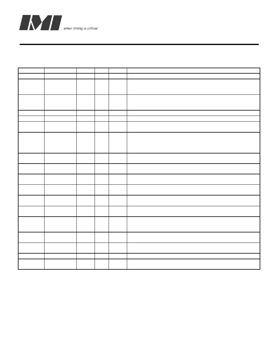
Pin Description
Pin No.
Pin Name
PWR
I/O
TYPE
Description
1,2,45
REF(0:2)
VDD
O
Buffer output clocks of the reference signal at Xin.
4
Xin
VDD
I
OSC
On-chip reference oscillator input pin. Requires either an
external parallel resonant crystal (nominally 14.318 MHz) or
externally generated reference signal
5
Xout
VDD
O
OSC
On-chip reference oscillator output pin. Drives an external
parallel resonant crystal. When an externally generated
reference signal is used at Xin, this pin remains unconnected.
6
S1
I
PD
Input for selecting CPU//PCI frequencies (see table 1,p.1).
18
S0
I
PU
Input for selecting CPU//PCI frequencies (see table 1,p.1).
8,9,11,12,
13,14,16
PCI_F,
PCI(0:5)
VDD
O
PCI clock outputs, synchronous to the CPU clocks. If PCI_STP#
is asserted low, PCI (0:5) stop in a low state, PCI_F does NOT.
19
SDATA
VDD
I/O
PU
Serial data input pin. Conforms to the Philips I2C specification of
a Slave Receiver device. This pin is an input when receiving
data. It is an open drain output when acknowledging. See I2C
function description, p.5.
20
SCLK
VDD
I
PU
Serial clock input pin. Conforms to the Philips I2C 100KHz
Specification.
22,23
24/48M
VDD
O
Programmable Peripheral clock outputs. Default to 48mhz for
USB, but can be programmed to 24MHz through I2C bus.
26
PCI_STP#
VDD
I
PU
Input pin for stopping PCI (0:5) when active low. Default high.
(see power management description p.3 )
27
CPU_STP#
VDD
I
PU
Input pin for stopping CPU (0:1) and AGP (0:1) when active low.
Default high. (see power management description p.3 )
29,30,32,3
3,35,36,38
SDRAM
(FB,0:5)
VDDS
O
SDRAM clock outputs. They are buffered outputs of the signal
applied at SDRAM_IN, pin39.
41,42
CPU(0:1)
VDDC
O
Host (CPU) Clock outputs. See Table 1,p.1 for frequency
selection.
44
PWR_DWN#
VDD
I
PU
Input pin for shutting down the device when asserted low. All
outputs, PLL’s and crystal are stopped for minimum power
consumption.
7,15,21,25
46, 48
VDD
-
P
-
3.3 Volt common power supply pins.
28,34
VDDS
-
P
-
3.3 Volt power supply pins for SDRAM_IN, SDRAM (FB, 0:5)
outputs.
40
VDDC
-
P
-
3.3 or 2.5 Volt power supply pins for the CPU (0:1), outputs.
3,10,17,24
,3137, 43
VSS
-
P
-
Common Ground pins.
Table 2
A bypass capacitor (0.1 uF) should be placed as close as possible to each Vdd, Vddc, and Vdds pins. If these
bypass capacitors are not close to the pins, their high frequency filtering characteristic will be canceled by the
lead inductance of the traces.
相关PDF资料 |
PDF描述 |
|---|---|
| IMIC9806CY | PROC SPECIFIC CLOCK GENERATOR, PDSO48 |
| IMIC9806IAT | PROC SPECIFIC CLOCK GENERATOR, PDSO48 |
| IMIFS782BZBT | 82 MHz, OTHER CLOCK GENERATOR, PDSO8 |
| IMIFS784BZBT | 82 MHz, OTHER CLOCK GENERATOR, PDSO8 |
| IMISC643AYB | PROC SPECIFIC CLOCK GENERATOR, PDSO48 |
相关代理商/技术参数 |
参数描述 |
|---|---|
| IMIC9806JBT | 制造商:Cypress Semiconductor 功能描述:Development Tools, Notebook, Intel Piii /Celeron 制造商:Rochester Electronics LLC 功能描述:- Bulk |
| IMIC9812DYBD | 制造商:IMI 功能描述: |
| IMIC9827H | 制造商:未知厂家 制造商全称:未知厂家 功能描述:Clocks and Buffers |
| IMIC9827JT | 制造商:Rochester Electronics LLC 功能描述:TIMING DEVICE - Tape and Reel |
| IMIC9827JTT | 制造商:Rochester Electronics LLC 功能描述:TIMING DEVICE - Bulk |
发布紧急采购,3分钟左右您将得到回复。