- 您现在的位置:买卖IC网 > PDF目录67720 > IMIC9806CY (CYPRESS SEMICONDUCTOR CORP) PROC SPECIFIC CLOCK GENERATOR, PDSO48 PDF资料下载
参数资料
| 型号: | IMIC9806CY |
| 厂商: | CYPRESS SEMICONDUCTOR CORP |
| 元件分类: | 时钟产生/分配 |
| 英文描述: | PROC SPECIFIC CLOCK GENERATOR, PDSO48 |
| 封装: | SSOP-48 |
| 文件页数: | 14/15页 |
| 文件大小: | 185K |
| 代理商: | IMIC9806CY |
C9806C
I
2C Frequency Clock Generator for Mobile Pentium II Applications.
Preliminary
INTERNATIONAL MICROCIRCUITS, INC. 525 LOS COCHES ST.
Rev.1.0
2/9/2000
MILPITAS, CA 95035. TEL: 408-263-6300. FAX 408-263-6571
Page 8 of 15
http://www.imicorp.com
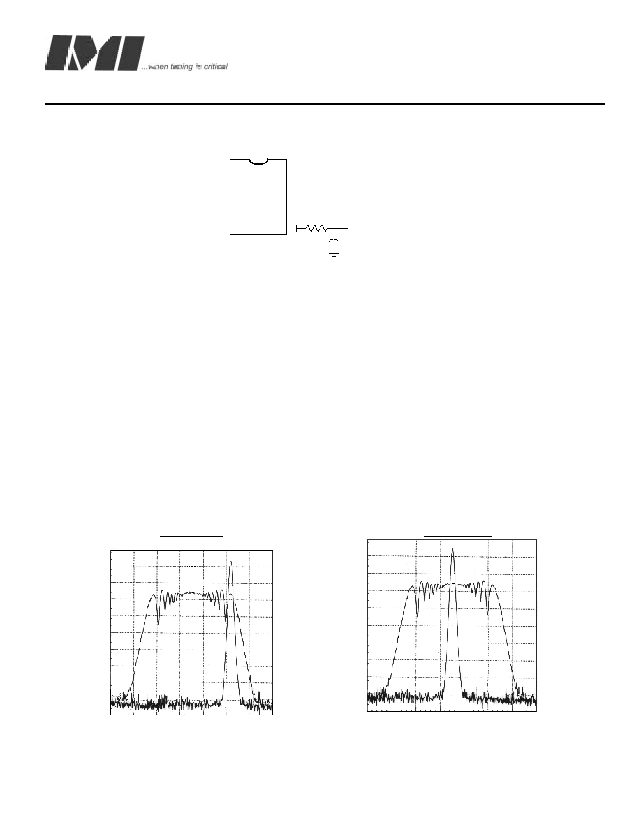
Reducing Clock Noise with Power Bypassing
Figure 4
The C9806C produces many different frequency clocks simultaneously. If these clocks are allowed to couple back into
the Internal Analog circuitry that may cause a destablizing noise injection condition. To eliminate this potential problem
and produce the cleanest design and clock outputs, IMI recommends bypassing the 3.3V VDD supply to the Analog
Power Pin (pin 25) with the circuitry shown in Figure 4. This will effectively isolate the device’s Analog Power Supply from
any noise that is present on it that will cause increased jitter and phase noise within it internal analog circuitry.
Spread Spectrum Clock Generation
(SSCG)
Spread Spectrum is a modulation technique applied here for maximum efficiency in minimizing Electro-Magnetic
Interference radiation generated from repetitive digital signals mainly clocks. A clock accumulates EM energy at the
center frequency it is generating. Spread Spectrum distributes this energy over a small frequency bandwidth therefore
spreading the same amount of energy over a spectrum. This technique is achieved by modulating the clock down from
or around the center of its resting frequency by a certain percentage (which also determines the energy distribution
bandwidth). In this device, Spread Spectrum is enabled by setting I2C byte0, bit1 = 1, and bit0 = 0. The default of the
device at power up keeps the Spread Spectrum disabled, it is therefore, important to have I2C accessibility to turn-on the
Spread Spectrum function. Once the Spread Spectrum is enabled, the spread bandwidth option is selected by SST (0:2)
in I2C byte 0, bits 4, 5 & 6 following table 5 below.
Down Spread
Center Spread
25
R
X
3.3 Volt VDD
.I nF
相关PDF资料 |
PDF描述 |
|---|---|
| IMIC9806IAT | PROC SPECIFIC CLOCK GENERATOR, PDSO48 |
| IMIFS782BZBT | 82 MHz, OTHER CLOCK GENERATOR, PDSO8 |
| IMIFS784BZBT | 82 MHz, OTHER CLOCK GENERATOR, PDSO8 |
| IMISC643AYB | PROC SPECIFIC CLOCK GENERATOR, PDSO48 |
| IMISC670DYB | PROC SPECIFIC CLOCK GENERATOR, PDSO48 |
相关代理商/技术参数 |
参数描述 |
|---|---|
| IMIC9806JBT | 制造商:Cypress Semiconductor 功能描述:Development Tools, Notebook, Intel Piii /Celeron 制造商:Rochester Electronics LLC 功能描述:- Bulk |
| IMIC9812DYBD | 制造商:IMI 功能描述: |
| IMIC9827H | 制造商:未知厂家 制造商全称:未知厂家 功能描述:Clocks and Buffers |
| IMIC9827JT | 制造商:Rochester Electronics LLC 功能描述:TIMING DEVICE - Tape and Reel |
| IMIC9827JTT | 制造商:Rochester Electronics LLC 功能描述:TIMING DEVICE - Bulk |
发布紧急采购,3分钟左右您将得到回复。