- 您现在的位置:买卖IC网 > PDF目录383110 > IP82C54 (HARRIS SEMICONDUCTOR) CMOS Programmable Interval Timer PDF资料下载
参数资料
| 型号: | IP82C54 |
| 厂商: | HARRIS SEMICONDUCTOR |
| 元件分类: | XO, clock |
| 英文描述: | CMOS Programmable Interval Timer |
| 中文描述: | 3 TIMER(S), PROGRAMMABLE TIMER, PDIP24 |
| 文件页数: | 8/17页 |
| 文件大小: | 142K |
| 代理商: | IP82C54 |
4-8
Both count and status of the selected counter(s) may be
latched simultaneously by setting both COUNT and STATUS
bits D5, D4 = 0. This is functionally the same as issuing two
separate read-back commands at once, and the above dis-
cussions apply here also. Specifically, if multiple count
and/or status read-back commands are issued to the same
counter(s) without any intervening reads, all but the first are
ignored. This is illustrated in Figure 7.
If both count and status of a counter are latched, the first
read operation of that counter will return latched status,
regardless of which was latched first. The next one or two
reads (depending on whether the counter is programmed for
one or two type counts) return latched count. Subsequent
reads return unlatched count.
Mode Definitions
The following are defined for use in describing the operation
of the 82C54.
CLK PULSE:
A rising edge, then a falling edge, in that order, of a
Counter’s CLK input.
TRIGGER:
A rising edge of a Counter’s Gate input.
COUNTER LOADING:
The transfer of a count from the CR to the CE (See “Func-
tional Description”)
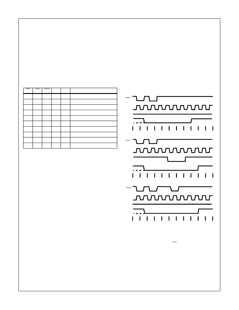
Mode 0: Interrupt on Terminal Count
Mode 0 is typically used for event counting. After the Control
Word is written, OUT is initially low, and will remain low until
the Counter reaches zero. OUT then goes high and remains
high until a new count or a new Mode 0 Control Word is writ-
ten to the Counter.
GATE = 1 enables counting; GATE = 0 disables counting.
GATE has no effect on OUT.
After the Control Word and initial count are written to a
Counter, the initial count will be loaded on the next CLK
pulse. This CLK pulse does not decrement the count, so for
an initial count of N, OUT does not go high until N + 1 CLK
pulses after the initial count is written.
If a new count is written to the Counter it will be loaded on
the next CLK pulse and counting will continue from the new
count. If a two-byte count is written, the following happens:
(1)Writing the first byte disables counting. Out is set low
immediately (no clock pulse required).
(2)Writing the second byte allows the new count to be
loaded on the next CLK pulse.
This allows the counting sequence to be synchronized by
software. Again OUT does not go high until N + 1 CLK
pulses after the new count of N is written.
If an initial count is written while GATE = 0, it will still be
loaded on the next CLK pulse. When GATE goes high, OUT
will go high N CLK pulses later; no CLK pulse is needed to
load the counter as this has already been done.
CW = 10
LSB = 4
FIGURE 9. MODE 0
NOTES: The following conventions apply to all mode timing diagrams.
1. Counters are programmed for binary (not BCD) counting and for
reading/writing least significant byte (LSB) only.
2. The counter is always selected (CS always low).
3. CW stands for “Control Word”; CW = 10 means a control word of
10, Hex is written to the counter.
4. LSB stands for Least significant “byte” of count.
5. Numbers below diagrams are count values. The lower number is
the least significant byte. The upper number is the most signifi-
cant byte. Since the counter is programmed to read/write LSB
only, the most significant byte cannot be read.
6. N stands for an undefined count.
7. Vertical lines show transitions between count values.
CS
RD
WR
A1
A0
0
1
0
0
0
Write into Counter 0
0
1
0
0
1
Write into Counter 1
0
1
0
1
0
Write into Counter 2
0
1
0
1
1
Write Control Word
0
0
1
0
0
Read from Counter 0
0
0
1
0
1
Read from Counter 1
0
0
1
1
0
Read from Counter 2
0
0
1
1
1
No-Operation (Three-State)
1
X
X
X
X
No-Operation (Three-State)
0
1
1
X
X
No-Operation (Three-State)
FIGURE 8. READ/WRITE OPERATIONS SUMMARY
WR
CLK
GATE
OUT
WR
CLK
GATE
OUT
WR
CLK
GATE
OUT
CW = 10
LSB = 3
CW = 10
LSB = 3
LSB = 2
N
N
N
N
0
4
0
3
0
2
0
1
0
0
FF
FF
FF
FE
N
N
N
N
0
3
0
2
0
2
0
2
0
1
0
0
FF
FF
N
N
N
N
0
3
0
2
0
1
0
2
0
1
0
0
FF
FF
82C54
相关PDF资料 |
PDF描述 |
|---|---|
| IP82C54-10 | CMOS Programmable Interval Timer |
| IP82C59A | CMOS Priority Interrupt Controller |
| IP82C59A-5 | CMOS Priority Interrupt Controller |
| IP82C59A-12 | CMOS Priority Interrupt Controller |
| IP82C83H | CMOS Octal Latching Inverting Bus Driver |
相关代理商/技术参数 |
参数描述 |
|---|---|
| IP82C54/+ | 制造商:未知厂家 制造商全称:未知厂家 功能描述:Analog Timer Circuit |
| IP82C54-10 | 功能描述:计时器和支持产品 PERIPH PRG-CNTR 5V 10MHZ 24PDIP IND RoHS:否 制造商:Micrel 类型:Standard 封装 / 箱体:SOT-23 内部定时器数量:1 电源电压-最大:18 V 电源电压-最小:2.7 V 最大功率耗散: 最大工作温度:+ 85 C 最小工作温度:- 40 C 封装:Reel |
| IP82C54-10S5001 | 制造商:Rochester Electronics LLC 功能描述:- Bulk |
| IP82C54-10Z | 功能描述:计时器和支持产品 W/ANNEAL PERIPH PRG- CNTR 5V 10MHZ 24PDIP RoHS:否 制造商:Micrel 类型:Standard 封装 / 箱体:SOT-23 内部定时器数量:1 电源电压-最大:18 V 电源电压-最小:2.7 V 最大功率耗散: 最大工作温度:+ 85 C 最小工作温度:- 40 C 封装:Reel |
| IP82C54-12 | 制造商:INTERSIL 制造商全称:Intersil Corporation 功能描述:CMOS Programmable Interval Timer |
发布紧急采购,3分钟左右您将得到回复。