- 您现在的位置:买卖IC网 > PDF目录377504 > IRF530NSPBF (International Rectifier) HEXFET Power MOSFET PDF资料下载
参数资料
| 型号: | IRF530NSPBF |
| 厂商: | International Rectifier |
| 英文描述: | HEXFET Power MOSFET |
| 中文描述: | HEXFET功率MOSFET |
| 文件页数: | 2/10页 |
| 文件大小: | 283K |
| 代理商: | IRF530NSPBF |
2
www.irf.com
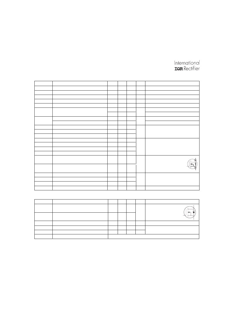
S
D
G
Parameter
Min. Typ. Max. Units
Conditions
I
S
Continuous Source Current
(Body Diode)
Pulsed Source Current
(Body Diode)
Diode Forward Voltage
Reverse Recovery Time
Reverse Recovery Charge
Forward Turn-On Time
MOSFET symbol
showing the
integral reverse
p-n junction diode.
T
J
= 25°C, I
S
= 9.0A, V
GS
= 0V
T
J
= 25°C, I
F
= 9.0A
di/dt = 100A/μs
–––
–––
I
SM
–––
–––
V
SD
t
rr
Q
rr
t
on
–––
–––
–––
–––
93
320
1.3
140
480
V
ns
nC
Intrinsic turn-on time is negligible (turn-on is dominated by L
S
+L
D
)
Source-Drain Ratings and Characteristics
17
60
Repetitive rating; pulse width limited by
max. junction temperature. (See fig. 11)
Starting T
J
= 25°C, L = 2.3mH
R
G
= 25
, I
AS
= 9.0A, V
GS
=10V (See Figure 12)
I
SD
≤
9.0A di/d
≤
410A/μs, V
DD
≤
V
(BR)DSS
,
T
J
≤
175°C
Pulse width
≤
400μs; duty cycle
≤
2%.
This is a typical value at device destruction and represents
operation outside rated limits.
This is a calculated value limited to T
J
= 175°C .
Uses IRF530N data and test conditions.
**When mounted on 1" square PCB (FR-4 or G-10 Material). For
recommended footprint and soldering techniques refer to
application note #AN-994
Parameter
Min. Typ. Max. Units
100
–––
–––
0.11
–––
–––
2.0
–––
12
–––
–––
–––
–––
–––
–––
–––
–––
–––
–––
–––
–––
–––
–––
–––
–––
9.2
–––
22
–––
35
–––
25
Conditions
V
GS
= 0V, I
D
= 250μA
Reference to 25°C, I
D
= 1mA
V
GS
= 10V, I
D
= 9.0A
V
DS
= V
GS
, I
D
= 250μA
V
DS
= 50V, I
D
= 9.0A
V
DS
= 100V, V
GS
= 0V
V
DS
= 80V, V
GS
= 0V, T
J
= 150°C
V
GS
= 20V
V
GS
= -20V
I
D
= 9.0A
V
DS
= 80V
V
GS
= 10V, See Fig. 6 and 13
V
DD
= 50V
I
D
= 9.0A
R
G
= 12
V
GS
= 10V, See Fig. 10
Between lead,
6mm (0.25in.)
from package
and center of die contact
V
GS
= 0V
V
DS
= 25V
= 1.0MHz, See Fig. 5
I
AS
= 9.0A, L = 2.3mH
V
(BR)DSS
V
(BR)DSS
/
T
J
Breakdown Voltage Temp. Coefficient
R
DS(on)
Static Drain-to-Source On-Resistance
V
GS(th)
Gate Threshold Voltage
g
fs
Forward Transconductance
Drain-to-Source Breakdown Voltage
–––
–––
90
4.0
–––
25
250
100
-100
37
7.2
11
–––
–––
–––
–––
V
V/°C
m
V
S
μA
Gate-to-Source Forward Leakage
Gate-to-Source Reverse Leakage
Total Gate Charge
Gate-to-Source Charge
Gate-to-Drain ("Miller") Charge
Turn-On Delay Time
Rise Time
Turn-Off Delay Time
Fall Time
nA
Q
g
Q
gs
Q
gd
t
d(on)
t
r
t
d(off)
t
f
nC
–––
–––
C
iss
C
oss
C
rss
E
AS
Input Capacitance
Output Capacitance
Reverse Transfer Capacitance
Single Pulse Avalanche Energy
–––
–––
–––
–––
920
130
19
340
–––
–––
–––
93
pF
mJ
nH
Electrical Characteristics @ T
J
= 25°C (unless otherwise specified)
L
D
Internal Drain Inductance
L
S
Internal Source Inductance
–––
–––
S
D
G
I
GSS
ns
I
DSS
Drain-to-Source Leakage Current
相关PDF资料 |
PDF描述 |
|---|---|
| IRF530N | Power MOSFET(Vdss=100V, Rds(on)=90mohm, Id=17A) |
| IRF530N | 22A, 100V, 0.064 Ohm, N-Channel Power MOSFET |
| IRF530S | Power MOSFET(Vdss=100V, Rds(on)=0.16ohm, Id=14A) |
| IRF540PBF | HEXFET㈢ Power MOSFET |
| IRF540SPBF | HEXFET㈢ Power MOSFET |
相关代理商/技术参数 |
参数描述 |
|---|---|
| IRF530NSTRL | 制造商:International Rectifier 功能描述: |
| IRF530NSTRLHR | 制造商:International Rectifier 功能描述:Trans MOSFET N-CH 100V 17A 3-Pin(2+Tab) D2PAK T/R |
| IRF530NSTRLPBF | 功能描述:MOSFET MOSFT 100V 17A 90mOhm 24.7nC RoHS:否 制造商:STMicroelectronics 晶体管极性:N-Channel 汲极/源极击穿电压:650 V 闸/源击穿电压:25 V 漏极连续电流:130 A 电阻汲极/源极 RDS(导通):0.014 Ohms 配置:Single 最大工作温度: 安装风格:Through Hole 封装 / 箱体:Max247 封装:Tube |
| IRF530NSTRRHR | 制造商:International Rectifier 功能描述:Trans MOSFET N-CH 100V 17A 3-Pin(2+Tab) D2PAK T/R |
| IRF530NSTRRPBF | 功能描述:MOSFET 100V 1 N-CH HEXFET 90mOhms 24.7nC RoHS:否 制造商:STMicroelectronics 晶体管极性:N-Channel 汲极/源极击穿电压:650 V 闸/源击穿电压:25 V 漏极连续电流:130 A 电阻汲极/源极 RDS(导通):0.014 Ohms 配置:Single 最大工作温度: 安装风格:Through Hole 封装 / 箱体:Max247 封装:Tube |
发布紧急采购,3分钟左右您将得到回复。