- 您现在的位置:买卖IC网 > PDF目录17685 > IRF6603 (International Rectifier)MOSFET N-CH 30V 27A DIRECTFET PDF资料下载
参数资料
| 型号: | IRF6603 |
| 厂商: | International Rectifier |
| 文件页数: | 8/12页 |
| 文件大小: | 0K |
| 描述: | MOSFET N-CH 30V 27A DIRECTFET |
| 其它有关文件: | DirectFET MOSFET 4Ps Checklist |
| 产品变化通告: | (EP) Parts Discontinuation 25/May/2012 |
| 产品目录绘图: | IR Hexfet Circuit |
| 标准包装: | 1 |
| 系列: | HEXFET® |
| FET 型: | MOSFET N 通道,金属氧化物 |
| FET 特点: | 逻辑电平门 |
| 漏极至源极电压(Vdss): | 30V |
| 电流 - 连续漏极(Id) @ 25° C: | 27A |
| 开态Rds(最大)@ Id, Vgs @ 25° C: | 3.4 毫欧 @ 25A,10V |
| Id 时的 Vgs(th)(最大): | 2.5V @ 250µA |
| 闸电荷(Qg) @ Vgs: | 72nC @ 4.5V |
| 输入电容 (Ciss) @ Vds: | 6590pF @ 15V |
| 功率 - 最大: | 3.6W |
| 安装类型: | 表面贴装 |
| 封装/外壳: | DirectFET? 等容 MT |
| 供应商设备封装: | DIRECTFET? MT |
| 包装: | 剪切带 (CT) |
| 其它名称: | *IRF6603 IRF6603CT |
�� �
�
�IRF6603�
�Power� MOSFET� Selection� for� Non-Isolated� DC/DC� Converters�
�P� loss� =� P� conduction� +� P� drive� +� P� output�
�(� )�
�P� loss� =� I� rms� � R� ds(on)�
�+� ?� oss� � V� in� � f� +� (� Q� rr� � V� in� � f� )�
�Control FET�
�Special� attention� has� been� given� to� the� power� losses�
�in� the� switching� elements� of� the� circuit� -� Q1� and� Q2.�
�Power� losses� in� the� high� side� switch� Q1,� also� called�
�the� Control� FET,� are� impacted� by� the� R� ds(on)� of� the�
�MOSFET,� but� these� conduction� losses� are� only� about�
�one� half� of� the� total� losses.�
�Power� losses� in� the� control� switch� Q1� are� given�
�by;�
�P� loss� =� P� conduction� +� P� switching� +� P� drive� +� P� output�
�This� can� be� expanded� and� approximated� by;�
�Synchronous� FET�
�The� power� loss� equation� for� Q2� is� approximated�
�by;�
�*�
�2�
�+� (� Q� g� � V� g� � f� )�
�?� Q� ?�
�?� 2� ?�
�P� loss� =� (� I� rms� � R� ds(on� )� )�
�� V� in� � f� ?�
�2�
�?� Q� gd� ?� ?�
�+� ?� I� � � V� in� � f� ?� +� ?� I� �
�?� i� g� ?� ?�
�Q� gs� 2�
�i� g�
�?�
�?�
�*dissipated� primarily� in� Q1.�
�For� the� synchronous� MOSFET� Q2,� R� ds(on)� is� an� im-�
�portant� characteristic;� however,� once� again� the� im-�
�portance� of� gate� charge� must� not� be� overlooked� since�
�it� impacts� three� critical� areas.� Under� light� load� the�
�� V� in� � f� ?�
�?� Q� oss�
�?� 2�
�?�
�+� (� Q� g� � V� g� � f� )�
�+�
�This� simplified� loss� equation� includes� the� terms� Q� gs2�
�and� Q� oss� which� are� new� to� Power� MOSFET� data� sheets.�
�Q� gs2� is� a� sub� element� of� traditional� gate-source�
�charge� that� is� included� in� all� MOSFET� data� sheets.�
�The� importance� of� splitting� this� gate-source� charge�
�into� two� sub� elements,� Q� gs1� and� Q� gs2� ,� can� be� seen� from�
�Fig� 16.�
�Q� gs2� indicates� the� charge� that� must� be� supplied� by�
�the� gate� driver� between� the� time� that� the� threshold�
�voltage� has� been� reached� and� the� time� the� drain� cur-�
�rent� rises� to� I� dmax� at� which� time� the� drain� voltage� be-�
�gins� to� change.� Minimizing� Q� gs2� is� a� critical� factor� in�
�reducing� switching� losses� in� Q1.�
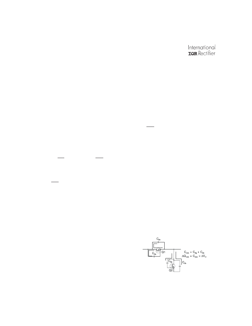
�Q� oss� is� the� charge� that� must� be� supplied� to� the� out-�
�put� capacitance� of� the� MOSFET� during� every� switch-�
�ing� cycle.� Figure� A� shows� how� Q� oss� is� formed� by� the�
�parallel� combination� of� the� voltage� dependant� (non-�
�linear)� capacitance?s� C� ds� and� C� dg� when� multiplied� by�
�the� power� supply� input� buss� voltage.�
�MOSFET� must� still� be� turned� on� and� off� by� the� con-�
�trol� IC� so� the� gate� drive� losses� become� much� more�
�significant.� Secondly,� the� output� charge� Q� oss� and� re-�
�verse� recovery� charge� Q� rr� both� generate� losses� that�
�are� transfered� to� Q1� and� increase� the� dissipation� in�
�that� device.� Thirdly,� gate� charge� will� impact� the�
�MOSFETs’� susceptibility� to� Cdv/dt� turn� on.�
�The� drain� of� Q2� is� connected� to� the� switching� node�
�of� the� converter� and� therefore� sees� transitions� be-�
�tween� ground� and� V� in� .� As� Q1� turns� on� and� off� there� is�
�a� rate� of� change� of� drain� voltage� dV/dt� which� is� ca-�
�pacitively� coupled� to� the� gate� of� Q2� and� can� induce�
�a� voltage� spike� on� the� gate� that� is� sufficient� to� turn�
�the� MOSFET� on,� resulting� in� shoot-through� current� .�
�The� ratio� of� Q� gd� /Q� gs1� must� be� minimized� to� reduce� the�
�potential� for� Cdv/dt� turn� on.�
�8�
�Figure� A:� Q� oss� Characteristic�
�www.irf.com�
�相关PDF资料 |
PDF描述 |
|---|---|
| UB16NBKW015D-DD | SWITCH PUSHBUTTON SPDT 5A 125V |
| 3386F-1-202T | TRIMMER 2K OHM 0.5W TH |
| 84BLN-BB2-014DN | KEYPAD BACKLIT RUBBER 4X4 LO PRO |
| KB16RKG01-12-CC | SWITCH PUSH SPDT 0.4VA 28V |
| MB2461A2W30 | SWITCH PUSHBUTTON DPDT 3A 125V |
相关代理商/技术参数 |
参数描述 |
|---|---|
| IRF6603TR1 | 功能描述:MOSFET 30V 1 N-CH HEXFET 8.1mOhms 11nC RoHS:否 制造商:STMicroelectronics 晶体管极性:N-Channel 汲极/源极击穿电压:650 V 闸/源击穿电压:25 V 漏极连续电流:130 A 电阻汲极/源极 RDS(导通):0.014 Ohms 配置:Single 最大工作温度: 安装风格:Through Hole 封装 / 箱体:Max247 封装:Tube |
| IRF6604 | 功能描述:MOSFET RoHS:否 制造商:STMicroelectronics 晶体管极性:N-Channel 汲极/源极击穿电压:650 V 闸/源击穿电压:25 V 漏极连续电流:130 A 电阻汲极/源极 RDS(导通):0.014 Ohms 配置:Single 最大工作温度: 安装风格:Through Hole 封装 / 箱体:Max247 封装:Tube |
| IRF6604TR1 | 功能描述:MOSFET RoHS:否 制造商:STMicroelectronics 晶体管极性:N-Channel 汲极/源极击穿电压:650 V 闸/源击穿电压:25 V 漏极连续电流:130 A 电阻汲极/源极 RDS(导通):0.014 Ohms 配置:Single 最大工作温度: 安装风格:Through Hole 封装 / 箱体:Max247 封装:Tube |
| IRF6607 | 功能描述:MOSFET RoHS:否 制造商:STMicroelectronics 晶体管极性:N-Channel 汲极/源极击穿电压:650 V 闸/源击穿电压:25 V 漏极连续电流:130 A 电阻汲极/源极 RDS(导通):0.014 Ohms 配置:Single 最大工作温度: 安装风格:Through Hole 封装 / 箱体:Max247 封装:Tube |
| IRF6607TR1 | 功能描述:MOSFET RoHS:否 制造商:STMicroelectronics 晶体管极性:N-Channel 汲极/源极击穿电压:650 V 闸/源击穿电压:25 V 漏极连续电流:130 A 电阻汲极/源极 RDS(导通):0.014 Ohms 配置:Single 最大工作温度: 安装风格:Through Hole 封装 / 箱体:Max247 封装:Tube |
发布紧急采购,3分钟左右您将得到回复。