- 您现在的位置:买卖IC网 > PDF目录384498 > IRFU3910 (International Rectifier) RECTIFIER SCHOTTKY SINGLE 5A 60V 100A-Ifsm 0.66Vf 0.2A-IR POWERMITE-3 5K/REEL PDF资料下载
参数资料
| 型号: | IRFU3910 |
| 厂商: | International Rectifier |
| 英文描述: | RECTIFIER SCHOTTKY SINGLE 5A 60V 100A-Ifsm 0.66Vf 0.2A-IR POWERMITE-3 5K/REEL |
| 中文描述: | 功率MOSFET(减振钢板基本\u003d 100V的时,RDS \u003d 0.115ohm,身份证\u003d 16A条) |
| 文件页数: | 2/10页 |
| 文件大小: | 141K |
| 代理商: | IRFU3910 |
IRFR/U3910
2
www.irf.com
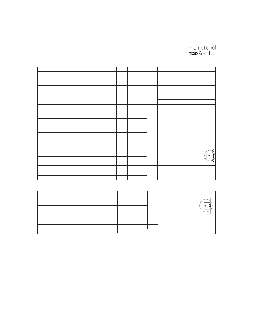
Parameter
Min.
100
–––
–––
2.0
6.4
–––
–––
–––
–––
–––
–––
–––
–––
–––
–––
–––
Typ. Max. Units
–––
–––
0.12
–––
––– 0.115
–––
4.0
–––
–––
–––
25
–––
250
–––
100
–––
-100
–––
44
–––
6.2
–––
21
6.4
–––
27
–––
37
–––
25
–––
Conditions
V
(BR)DSS
V
(BR)DSS
/
T
J
Breakdown Voltage Temp. Coefficient
R
DS(on)
Static Drain-to-Source On-Resistance
Drain-to-Source Breakdown Voltage
V
V
GS
= 0V, I
D
= 250μA
Reference to 25°C, I
D
= 1mA
V
GS
= 10V, I
D
= 10A
V
DS
= V
GS
, I
D
= 250μA
V
DS
= 50V, I
D
= 9.0A
V
DS
= 100V, V
GS
= 0V
V
DS
= 80V, V
GS
= 0V, T
J
= 150°C
V
GS
= 20V
V
GS
= -20V
I
D
= 9.0A
V
DS
= 80V
V
GS
= 10V, See Fig. 6 and 13
V
DD
= 50V
I
D
= 9.0A
R
G
= 12
R
D
= 5.5
,
See Fig. 10
Between lead,
6mm (0.25in.)
from package
and center of die contact
V
GS
= 0V
V
DS
= 25V
= 1.0MHz, See Fig. 5
V/°C
V
GS(th)
g
fs
Gate Threshold Voltage
Forward Transconductance
V
S
μA
Gate-to-Source Forward Leakage
Gate-to-Source Reverse Leakage
Total Gate Charge
Gate-to-Source Charge
Gate-to-Drain ("Miller") Charge
Turn-On Delay Time
Rise Time
Turn-Off Delay Time
Fall Time
nA
Q
g
Q
gs
Q
gd
t
d(on)
t
r
t
d(off)
t
f
nC
ns
C
iss
C
oss
C
rss
Input Capacitance
Output Capacitance
Reverse Transfer Capacitance
–––
–––
–––
640
160
88
–––
–––
–––
pF
Electrical Characteristics @ T
J
= 25°C (unless otherwise specified)
nH
I
GSS
S
D
G
L
S
Internal Source Inductance
–––
7.5
–––
L
D
Internal Drain Inductance
–––
4.5 –––
I
DSS
Drain-to-Source Leakage Current
S
D
G
Parameter
Min. Typ. Max. Units
Conditions
MOSFET symbol
showing the
integral reverse
p-n junction diode.
T
J
= 25°C, I
S
= 9.0A, V
GS
= 0V
T
J
= 25°C, I
F
= 9.0A
di/dt = 100A/μs
I
S
Continuous Source Current
(Body Diode)
Pulsed Source Current
(Body Diode)
Diode Forward Voltage
Reverse Recovery Time
Reverse RecoveryCharge
Forward Turn-On Time
–––
–––
I
SM
–––
–––
V
SD
t
rr
Q
rr
t
on
–––
–––
–––
–––
130
650
1.3
190
970
V
ns
nC
Intrinsic turn-on time is negligible (turn-on is dominated by L
S
+L
D
)
Source-Drain Ratings and Characteristics
A
16
60
Notes:
Repetitive rating; pulse width limited by
max. junction temperature. ( See fig. 11 )
V
DD
= 25V, starting T
J
= 25°C, L = 3.1mH
R
G
= 25
, I
AS
= 9.0A. (See Figure 12)
I
SD
≤
9.0A, di/dt
≤
520A/μs, V
DD
≤
V
(BR)DSS
,
T
J
≤
175°C
** When mounted on 1" square PCB (FR-4 or G-10 Material ) .
For recommended footprint and soldering techniques refer to application note #AN-994
Uses IRF530N data and test conditions
This is applied for I-PAK, Ls of D-PAK is measured between lead and
center of die contact
Pulse width
≤
300μs; duty cycle
≤
2%
相关PDF资料 |
PDF描述 |
|---|---|
| IRFRU5505 | 30V N-Channel PowerTrench MOSFET |
| IRFU5505 | 30V N-Channel PowerTrench MOSFET |
| IRFR5505 | P Channel Surface Mount HEXFET Power MOSFET(P沟道表贴型HEXFET功率MOS场效应管) |
| IRFRU6215 | Power MOSFET(Vdss=-150V, Rds(on)=0.295ohm, Id=-13A) |
| IRFU6215 | CAP 0.22UF 25V 10% X7R SMD-1206 TR-7-PL 3K/REEL |
相关代理商/技术参数 |
参数描述 |
|---|---|
| IRFU3910HR | 制造商:International Rectifier 功能描述:Trans MOSFET N-CH 100V 16A 3-Pin(3+Tab) TO-251 |
| IRFU3910PBF | 功能描述:MOSFET MOSFT 100V 15A 115mOhm 29.3nC RoHS:否 制造商:STMicroelectronics 晶体管极性:N-Channel 汲极/源极击穿电压:650 V 闸/源击穿电压:25 V 漏极连续电流:130 A 电阻汲极/源极 RDS(导通):0.014 Ohms 配置:Single 最大工作温度: 安装风格:Through Hole 封装 / 箱体:Max247 封装:Tube |
| IRFU3911 | 制造商:IRF 制造商全称:International Rectifier 功能描述:SMPS MOSFET |
| IRFU3911PBF | 功能描述:MOSFET N-CH 100V 14A I-PAK RoHS:是 类别:分离式半导体产品 >> FET - 单 系列:HEXFET® 标准包装:1,000 系列:MESH OVERLAY™ FET 型:MOSFET N 通道,金属氧化物 FET 特点:逻辑电平门 漏极至源极电压(Vdss):200V 电流 - 连续漏极(Id) @ 25° C:18A 开态Rds(最大)@ Id, Vgs @ 25° C:180 毫欧 @ 9A,10V Id 时的 Vgs(th)(最大):4V @ 250µA 闸电荷(Qg) @ Vgs:72nC @ 10V 输入电容 (Ciss) @ Vds:1560pF @ 25V 功率 - 最大:40W 安装类型:通孔 封装/外壳:TO-220-3 整包 供应商设备封装:TO-220FP 包装:管件 |
| IRFU410 | 制造商:INTERSIL 制造商全称:Intersil Corporation 功能描述:1.5A, 500V, 7.000 Ohm, N-Channel Power MOSFETs |
发布紧急采购,3分钟左右您将得到回复。