- 您现在的位置:买卖IC网 > PDF目录21664 > IRL5602S (International Rectifier)MOSFET P-CH 20V 24A D2PAK PDF资料下载
参数资料
| 型号: | IRL5602S |
| 厂商: | International Rectifier |
| 文件页数: | 2/9页 |
| 文件大小: | 0K |
| 描述: | MOSFET P-CH 20V 24A D2PAK |
| 标准包装: | 50 |
| 系列: | HEXFET® |
| FET 型: | MOSFET P 通道,金属氧化物 |
| FET 特点: | 逻辑电平门 |
| 漏极至源极电压(Vdss): | 20V |
| 电流 - 连续漏极(Id) @ 25° C: | 24A |
| 开态Rds(最大)@ Id, Vgs @ 25° C: | 42 毫欧 @ 12A,4.5V |
| Id 时的 Vgs(th)(最大): | 1V @ 250µA |
| 闸电荷(Qg) @ Vgs: | 44nC @ 4.5V |
| 输入电容 (Ciss) @ Vds: | 1460pF @ 15V |
| 功率 - 最大: | 75W |
| 安装类型: | 表面贴装 |
| 封装/外壳: | TO-263-3,D²Pak(2 引线+接片),TO-263AB |
| 供应商设备封装: | D2PAK |
| 包装: | 管件 |
| 其它名称: | *IRL5602S Q803261 |
�� �
�
�IRL5602S�
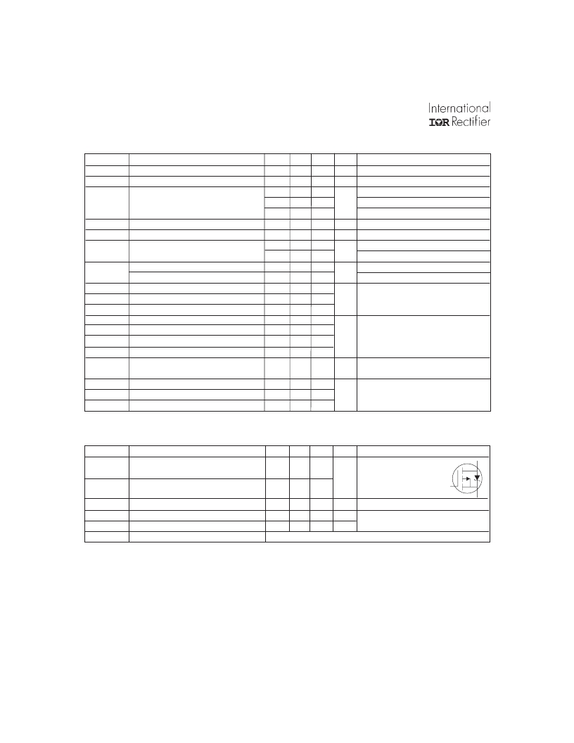
�Electrical� Characteristics� @� T� J� =� 25°C� (unless� otherwise� specified)�
�Parameter�
�Min.�
�Typ.� Max.� Units�
�Conditions�
�V� (BR)DSS�
�Drain-to-Source� Breakdown� Voltage�
�-20�
�–––� –––� V� V� GS� =� 0V,� I� D� =� -250μA�
�D� V� (BR)DSS� /� D� T� J�
�Breakdown� Voltage� Temp.� Coefficient�
�–––�
�-0.013� –––�
�V/°C� Reference� to� 25°C,� I� D� =� -1mA� ?�
�–––�
�–––� 0.042� V� GS� =� -4.5V,� I� D� =� -12A� ?�
�R� DS(on)�
�Static� Drain-to-Source� On-Resistance�
�–––�
�–––� 0.062�
�W�
�V� GS� =� -2.7V,� I� D� =� -10A�
�?�
�–––�
�–––� 0.075� V� GS� =� -2.5V,� I� D� =� -10A�
�?�
�μA�
�ns�
�V� GS(th)�
�g� fs�
�I� DSS�
�I� GSS�
�Q� g�
�Q� gs�
�Q� gd�
�t� d(on)�
�t� r�
�t� d(off)�
�t� f�
�Gate� Threshold� Voltage�
�Forward� Transconductance�
�Drain-to-Source� Leakage� Current�
�Gate-to-Source� Forward� Leakage�
�Gate-to-Source� Reverse� Leakage�
�Total� Gate� Charge�
�Gate-to-Source� Charge�
�Gate-to-Drain� ("Miller")� Charge�
�Turn-On� Delay� Time�
�Rise� Time�
�Turn-Off� Delay� Time�
�Fall� Time�
�-0.7�
�12�
�–––�
�–––�
�–––�
�–––�
�–––�
�–––�
�–––�
�–––�
�–––�
�–––�
�–––�
�–––� -1.0� V� V� DS� =� V� GS� ,� I� D� =� -250μA�
�–––� –––� S� V� DS� =� -15V,� I� D� =� -12A� ?�
�–––� -25� V� DS� =� -20V,� V� GS� =� 0V�
�–––� -250� V� DS� =� -16V,� V� GS� =� 0V,� T� J� =� 150°C�
�–––� 500� V� GS� =� -8.0V�
�nA�
�–––� -500� V� GS� =� 8.0V�
�–––� 44� I� D� =� -12A�
�–––� 8.7� nC� V� DS� =� -16V�
�–––� 19� V� GS� =� -4.5V,� See� Fig.� 6� and� 13� ??�
�9.7� –––� V� DD� =� -10� V�
�73� –––� I� D� =� -12A�
�53� –––� R� G� =� 6.0� W� ,� V� GS� =� 4.5V�
�84� –––� R� D� =� 0.8� W� ,� See� Fig.� 10� ??�
�L� S�
�Internal� Source� Inductance�
�–––�
�7.5�
�–––�
�nH�
�Between� lead,�
�and� center� of� die� contact�
�C� iss�
�C� oss�
�C� rss�
�Input� Capacitance�
�Output� Capacitance�
�Reverse� Transfer� Capacitance�
�–––�
�–––�
�–––�
�1460� –––� V� GS� =� 0V�
�790� –––� pF� V� DS� =� -15V�
�370� –––� ?� =� 1.0MHz,� See� Fig.� 5� ?�
�Source-Drain� Ratings� and� Characteristics�
�Parameter�
�Min.� Typ.� Max.� Units�
�Conditions�
�I� S�
�I� SM�
�Continuous� Source� Current�
�(Body� Diode)�
�Pulsed� Source� Current�
�(Body� Diode)� ?�
�–––� –––�
�–––� –––�
�-24�
�-96�
�A�
�MOSFET� symbol�
�showing� the�
�integral� reverse�
�p-n� junction� diode.�
�G�
�D�
�S�
�V� SD�
�Diode� Forward� Voltage�
�–––� –––� -1.4� V� T� J� =� 25°C,� I� S� =� -12A,� V� GS� =� 0V�
�?�
�t� rr�
�Q� rr�
�t� on�
�Notes:�
�Reverse� Recovery� Time�
�Reverse� RecoveryCharge�
�Forward� Turn-On� Time�
�–––� 58� 88� ns� T� J� =� 25°C,� I� F� =� -12A�
�–––� 54� 81� nC� di/dt� =� -100A/μs� ?�
�Intrinsic� turn-on� time� is� negligible� (turn-on� is� dominated� by� L� S� +L� D� )�
�?� Repetitive� rating;� pulse� width� limited� by�
�max.� junction� temperature.� (� See� fig.� 11� )�
�?� Starting� T� J� =� 25°C,� L� =� 3.0mH�
�R� G� =� 25� W� ,� I� AS� =� -14A.� (See� Figure� 12)�
�?� I� SD� £� -12A,� di/dt� £� 120A/μs,� V� DD� £� V� (BR)DSS� ,�
�T� J� £� 175°C�
�?� Pulse� width� £� 300μs;� duty� cycle� £� 2%.�
�**� When� mounted� on� FR-4� board� using� minimum� recommended� footprint.�
�For� recommended� footprint� and� soldering� techniques� refer� to� application� note� #AN-994.�
�2�
�www.irf.com�
�相关PDF资料 |
PDF描述 |
|---|---|
| AT3077A | SW CAP SQUARE BEVELED BLACK |
| IRL3502S | MOSFET N-CH 20V 110A D2PAK |
| IRFZ44NS | MOSFET N-CH 55V 49A D2PAK |
| AT3075F | CAP BEVELED GREEN FOR ILLUM UB2 |
| 3214G-1-200E | TRIMMER 20 OHM 0.25W SMD |
相关代理商/技术参数 |
参数描述 |
|---|---|
| IRL5602SHR | 制造商:International Rectifier 功能描述:Trans MOSFET P-CH 20V 24A 3-Pin(2+Tab) D2PAK |
| IRL5602SPBF | 功能描述:MOSFET 20V 1 N-CH HEXFET 42mOhms 29.3nC RoHS:否 制造商:STMicroelectronics 晶体管极性:N-Channel 汲极/源极击穿电压:650 V 闸/源击穿电压:25 V 漏极连续电流:130 A 电阻汲极/源极 RDS(导通):0.014 Ohms 配置:Single 最大工作温度: 安装风格:Through Hole 封装 / 箱体:Max247 封装:Tube |
| IRL5602SPBF | 制造商:International Rectifier 功能描述:MOSFET |
| IRL5602STRL | 功能描述:MOSFET P-CH 20V 24A D2PAK RoHS:否 类别:分离式半导体产品 >> FET - 单 系列:HEXFET® 标准包装:1,000 系列:MESH OVERLAY™ FET 型:MOSFET N 通道,金属氧化物 FET 特点:逻辑电平门 漏极至源极电压(Vdss):200V 电流 - 连续漏极(Id) @ 25° C:18A 开态Rds(最大)@ Id, Vgs @ 25° C:180 毫欧 @ 9A,10V Id 时的 Vgs(th)(最大):4V @ 250µA 闸电荷(Qg) @ Vgs:72nC @ 10V 输入电容 (Ciss) @ Vds:1560pF @ 25V 功率 - 最大:40W 安装类型:通孔 封装/外壳:TO-220-3 整包 供应商设备封装:TO-220FP 包装:管件 |
| IRL5602STRLHR | 制造商:International Rectifier 功能描述:Trans MOSFET P-CH 20V 24A 3-Pin(2+Tab) D2PAK T/R |
发布紧急采购,3分钟左右您将得到回复。