- 您现在的位置:买卖IC网 > PDF目录360969 > IRLP2505 PDF资料下载
参数资料
| 型号: | IRLP2505 |
| 文件页数: | 2/8页 |
| 文件大小: | 148K |
| 代理商: | IRLP2505 |
IRLP2505
Parameter
Min. Typ. Max. Units
55
–––
–––
0.035 –––
–––
––– 0.008
–––
––– 0.010
–––
––– 0.013
1.0
–––
59
–––
–––
–––
–––
–––
–––
–––
–––
–––
–––
–––
–––
–––
–––
–––
–––
12
–––
160
–––
43
–––
84
Conditions
V
GS
= 0V, I
D
= 250μA
Reference to 25°C, I
D
= 1mA
V
GS
= 10V, I
D
= 54A
V
GS
= 5.0V, I
D
= 54A
V
GS
= 4.0V, I
D
= 45A
V
DS
= V
GS
, I
D
= 250μA
V
DS
= 25V, I
D
= 54A
V
DS
= 55V, V
GS
= 0V
V
DS
= 44V, V
GS
= 0V, T
J
= 150°C
V
GS
= 20V
V
GS
= -20V
I
D
= 54A
V
DS
= 44V
V
GS
= 5.0V, See Fig. 6 and 13
V
DD
= 28V
I
D
= 54A
R
G
= 1.3
,
V
GS
= 5.0V
R
D
= 0.50
,
See Fig. 10
Between lead,
6mm (0.25in.)
from package
and center of die contact
V
GS
= 0V
V
DS
= 25V
= 1.0MHz, See Fig. 5
V
(BR)DSS
V
(BR)DSS
/
T
J
Breakdown Voltage Temp. Coefficient
Drain-to-Source Breakdown Voltage
–––
V
V/°C
V
GS(th)
g
fs
Gate Threshold Voltage
Forward Transconductance
2.0
–––
25
250
100
-100
130
25
67
–––
–––
–––
–––
V
S
Gate-to-Source Forward Leakage
Gate-to-Source Reverse Leakage
Total Gate Charge
Gate-to-Source Charge
Gate-to-Drain ("Miller") Charge
Turn-On Delay Time
Rise Time
Turn-Off Delay Time
Fall Time
Q
g
Q
gs
Q
gd
t
d(on)
t
r
t
d(off)
t
f
nC
C
iss
C
oss
C
rss
Input Capacitance
Output Capacitance
Reverse Transfer Capacitance
–––
–––
–––
5000
1100
390
–––
–––
–––
pF
Electrical Characteristics @ T
J
= 25°C (unless otherwise specified)
I
DSS
Drain-to-Source Leakage Current
I
GSS
L
S
Internal Source Inductance
–––
13
–––
L
D
Internal Drain Inductance
–––
5.0
–––
μA
nA
ns
nH
R
DS(on)
Static Drain-to-Source On-Resistance
Parameter
Min. Typ. Max. Units
Conditions
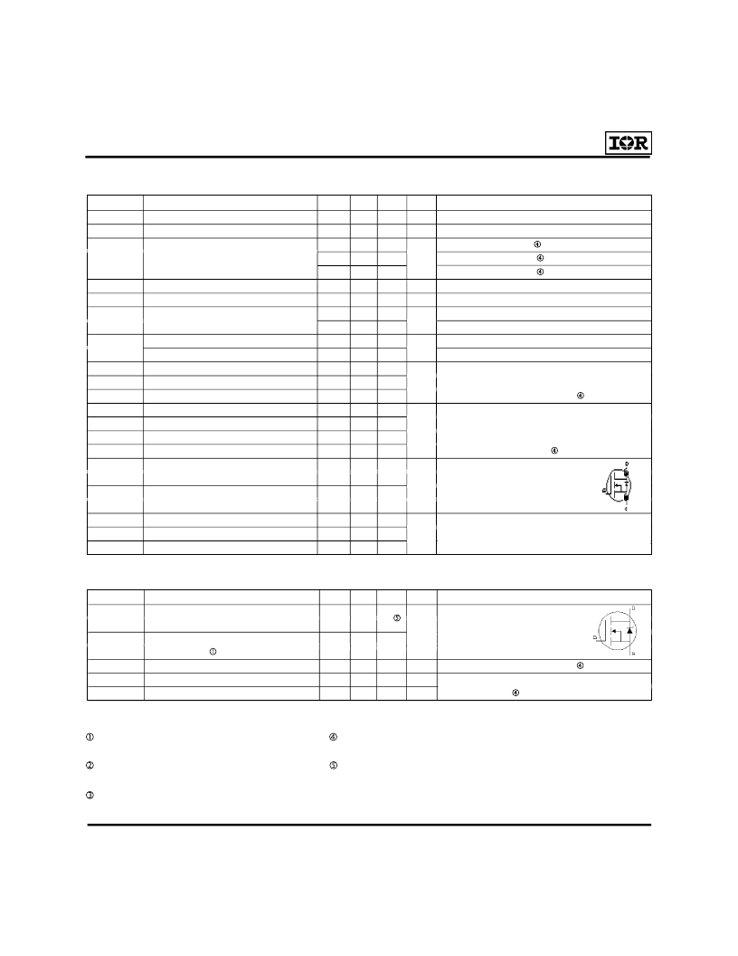
MOSFET symbol
showing the
integral reverse
p-n junction diode.
T
J
= 25°C, I
S
= 54A, V
GS
= 0V
T
J
= 25°C, I
F
= 54A
di/dt = 100A/μs
I
S
Continuous Source Current
(Body Diode)
Pulsed Source Current
(Body Diode)
Diode Forward Voltage
Reverse Recovery Time
Reverse RecoveryCharge
I
SM
V
SD
t
rr
Q
rr
–––
–––
–––
–––
140
650
1.3
210
970
V
ns
nC
Source-Drain Ratings and Characteristics
A
–––
–––
360
–––
–––
90
Repetitive rating; pulse width limited by
max. junction temperature. ( See fig. 11 )
Notes:
V
DD
= 25V, starting T
J
= 25°C, L = 240μH
R
G
= 25
, I
AS
= 54A. (See Figure 12)
I
SD
≤
54A, di/dt
≤
130A/μs, V
DD
≤
V
(BR)DSS
,
T
J
≤
175°C
Pulse width
≤
300μs; duty cycle
≤
2%.
Caculated continuous current based on maximum allowable
junction temperature;for recommended current-handling of the
package refer to Design Tip # 93-4
相关PDF资料 |
PDF描述 |
|---|---|
| IRLP2505 | HEXFET Power MOSFET(HEXFET 功率MOS场效应管) |
| IRLP3803 | TRANSISTOR | MOSFET | N-CHANNEL | 30V V(BR)DSS | 120A I(D) | TO-247AC |
| IRLR010 | TRANSISTOR | MOSFET | N-CHANNEL | 50V V(BR)DSS | 6.7A I(D) | TO-252 |
| IRLR014A | TRANSISTOR | MOSFET | N-CHANNEL | 60V V(BR)DSS | 8.2A I(D) | TO-252AA |
| IRLR020 | TRANSISTOR | MOSFET | N-CHANNEL | 50V V(BR)DSS | 14A I(D) | TO-252 |
相关代理商/技术参数 |
参数描述 |
|---|---|
| IRLP3034PBF | 功能描述:MOSFET MOSFT 40V 327A 1.7mOhm 108nC TO221 RoHS:否 制造商:STMicroelectronics 晶体管极性:N-Channel 汲极/源极击穿电压:650 V 闸/源击穿电压:25 V 漏极连续电流:130 A 电阻汲极/源极 RDS(导通):0.014 Ohms 配置:Single 最大工作温度: 安装风格:Through Hole 封装 / 箱体:Max247 封装:Tube |
| IRLP3803 | 制造商:未知厂家 制造商全称:未知厂家 功能描述:TRANSISTOR | MOSFET | N-CHANNEL | 30V V(BR)DSS | 120A I(D) | TO-247AC |
| IRLR 3110ZPBF | 制造商:International Rectifier 功能描述:Bulk |
| IRLR 3636PBF | 制造商:International Rectifier 功能描述:Bulk |
| IRLR/U120A | 制造商:FAIRCHILD 制造商全称:Fairchild Semiconductor 功能描述:ADVANCED POWER MOSFET |
发布紧急采购,3分钟左右您将得到回复。