- 您现在的位置:买卖IC网 > PDF目录79601 > IS80C52CXXX-16SHXXX:D (TEMIC SEMICONDUCTORS) 8-BIT, MROM, 16 MHz, MICROCONTROLLER, PQCC44 PDF资料下载
参数资料
| 型号: | IS80C52CXXX-16SHXXX:D |
| 厂商: | TEMIC SEMICONDUCTORS |
| 元件分类: | 微控制器/微处理器 |
| 英文描述: | 8-BIT, MROM, 16 MHz, MICROCONTROLLER, PQCC44 |
| 文件页数: | 107/310页 |
| 文件大小: | 4427K |
第1页第2页第3页第4页第5页第6页第7页第8页第9页第10页第11页第12页第13页第14页第15页第16页第17页第18页第19页第20页第21页第22页第23页第24页第25页第26页第27页第28页第29页第30页第31页第32页第33页第34页第35页第36页第37页第38页第39页第40页第41页第42页第43页第44页第45页第46页第47页第48页第49页第50页第51页第52页第53页第54页第55页第56页第57页第58页第59页第60页第61页第62页第63页第64页第65页第66页第67页第68页第69页第70页第71页第72页第73页第74页第75页第76页第77页第78页第79页第80页第81页第82页第83页第84页第85页第86页第87页第88页第89页第90页第91页第92页第93页第94页第95页第96页第97页第98页第99页第100页第101页第102页第103页第104页第105页第106页当前第107页第108页第109页第110页第111页第112页第113页第114页第115页第116页第117页第118页第119页第120页第121页第122页第123页第124页第125页第126页第127页第128页第129页第130页第131页第132页第133页第134页第135页第136页第137页第138页第139页第140页第141页第142页第143页第144页第145页第146页第147页第148页第149页第150页第151页第152页第153页第154页第155页第156页第157页第158页第159页第160页第161页第162页第163页第164页第165页第166页第167页第168页第169页第170页第171页第172页第173页第174页第175页第176页第177页第178页第179页第180页第181页第182页第183页第184页第185页第186页第187页第188页第189页第190页第191页第192页第193页第194页第195页第196页第197页第198页第199页第200页第201页第202页第203页第204页第205页第206页第207页第208页第209页第210页第211页第212页第213页第214页第215页第216页第217页第218页第219页第220页第221页第222页第223页第224页第225页第226页第227页第228页第229页第230页第231页第232页第233页第234页第235页第236页第237页第238页第239页第240页第241页第242页第243页第244页第245页第246页第247页第248页第249页第250页第251页第252页第253页第254页第255页第256页第257页第258页第259页第260页第261页第262页第263页第264页第265页第266页第267页第268页第269页第270页第271页第272页第273页第274页第275页第276页第277页第278页第279页第280页第281页第282页第283页第284页第285页第286页第287页第288页第289页第290页第291页第292页第293页第294页第295页第296页第297页第298页第299页第300页第301页第302页第303页第304页第305页第306页第307页第308页第309页第310页
195
7799D–AVR–11/10
ATmega8U2/16U2/32U2
Be sure to have interrupts enabled (WAKEUPE) to exit sleep mode
Put the MCU in sleep mode
Resuming the USB interface
Enable PLL
Wait PLL lock
Clear USB suspend clock
Clear Resume information
20.10 Registers Description
20.10.1
USBCON – USB General Control Registers
Bit 7 – USBE: USB macro Enable Bit
Writing this bit to one enables the USB controller and the USB data buffers (D+ and D-). Clear-
ing this bit disables the USB controller and buffers. When cleared the USB controller is reset.
Bit 6 – Res: Reserved
This bit is reserved and should always read as zero.
Bit 5 – FRZCLK: Freeze USB Clock Bit
Writing this bit to one disables the internal clock for the USB controller, and tehreby freezing it.
Activating this mode reduces power consumption. All the USB flags are kept unchanged. Only
the “Resume detection” is still active in this mode.
Writing this bit to zero unfreezes the USB controller and allows full operation of the USB
interface.
Bits 4:0 – Res: Reserved
These bits are reserved and should always read as zero.
20.10.2
UPOE – USB Software Output Enable register
Bit 7:6 – UPWE[1:0]: USB Buffers Direct Drive enable configuration
These bits select the mode of operation of the USB buffers according to Table 20-2. The possi-
ble configurations of these bits allows to enable or disable the USB buffers direct drive by soft-
ware. When direct drive for USB buffers is enable, the UPDRV[1:0] values are output to the
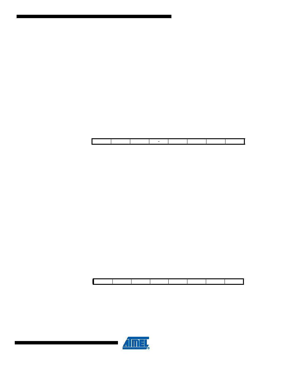
Bit
76543210
USBE
-
FRZLK
-
USBCON
Read/Write
R/W
R
R/W
R
Initial Value
0
1
0
Bit
7
6
5
4
3
2
1
0
UPWE1
UPWE0
UPDRV1
UPDRV0
-
DPI
DMI
UPOE
Read/Write
R/W
RRRR
Initial Value
0
相关PDF资料 |
PDF描述 |
|---|---|
| IS80C52EXXX-16SHXXX:R | 8-BIT, MROM, 16 MHz, MICROCONTROLLER, PQCC44 |
| IS80C52TXXX-25:R | 8-BIT, MROM, 25 MHz, MICROCONTROLLER, PQCC44 |
| IS80C52XXX-16:D | 8-BIT, MROM, 16 MHz, MICROCONTROLLER, PQCC44 |
| IF180C32-20:R | 8-BIT, 20 MHz, MICROCONTROLLER, PQFP44 |
| IF180C32-30:D | 8-BIT, 30 MHz, MICROCONTROLLER, PQFP44 |
相关代理商/技术参数 |
参数描述 |
|---|---|
| IS80C86 | 制造商:Rochester Electronics LLC 功能描述:- Bulk |
| IS80C86-2 | 制造商:Rochester Electronics LLC 功能描述:- Bulk |
| IS80C86-2R2490 | 制造商:Rochester Electronics LLC 功能描述:- Bulk |
| IS80C88 | 制造商:Rochester Electronics LLC 功能描述:- Bulk |
| IS80C88-2 | 制造商:Rochester Electronics LLC 功能描述:- Bulk |
发布紧急采购,3分钟左右您将得到回复。