- 您现在的位置:买卖IC网 > PDF目录11818 > IS82C52Z96 (Intersil)IC CTRLR CMOS SERIAL 28-PLCC PDF资料下载
参数资料
| 型号: | IS82C52Z96 |
| 厂商: | Intersil |
| 文件页数: | 14/20页 |
| 文件大小: | 0K |
| 描述: | IC CTRLR CMOS SERIAL 28-PLCC |
| 标准包装: | 750 |
| 特点: | 单芯片 UART/BRG |
| 通道数: | 1,UART |
| 规程: | RS232C |
| 电源电压: | 4.5 V ~ 5.5 V |
| 带并行端口: | 是 |
| 带故障启动位检测功能: | 是 |
| 带调制解调器控制功能: | 是 |
| 带CMOS: | 是 |
| 安装类型: | 表面贴装 |
| 封装/外壳: | 28-LCC(J 形引线) |
| 供应商设备封装: | 28-PLCC(11.51x11.51) |
| 包装: | 带卷 (TR) |
3
FN2950.3
April 26, 2006
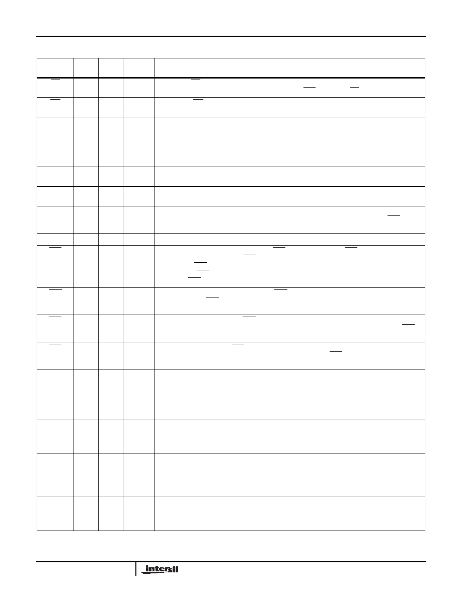
Pin Description
SYMBOL
PIN
NO.
TYPE
ACTIVE
LEVEL
DESCRIPTION
RD
1
I
Low
READ: The RD input causes the 82C52 to output data to the data bus (D0-D7). The data output
depends upon the state of the address inputs (A0-A1). CS0 enables the RD input.
WR
2
I
Low
WRITE: The WR input causes data from the data bus (D0-D7) to be input to the 82C52. Addressing
and chip select action is the same as for read operations.
D0-D7
3-10
I/O
High
DATA BITS 0-7: The Data Bus provides eight, three-state input/output lines for the transfer of data,
control and status information between the 82C52 and the CPU. For character formats of less than 8
bits, the corresponding D7, D6 and D5 are considered “don't cares” for data WRITE operations and
are 0 for data READ operations. These lines are normally in a high impedance state except during
read operations. D0 is the Least Significant Bit (LSB) and is the first serial data bit to be received or
transmitted.
A0, A1
11, 12
I
High
ADDRESS INPUTS: The address lines select the various internal registers during CPU bus
operations.
IX, OX
13, 14
I/O
CRYSTAL/CLOCK: Crystal connections for the internal Baud Rate Generator. IX can also be used
as an external clock input in which case OX should be left open.
SDO
15
O
High
SERIAL DATA OUTPUT: Serial data output from the 82C52 transmitter circuitry. A Mark (1) is a logic
one (high) and Space (0) is logic zero (low). SD0 is held in the Mark condition when CTS is false,
when RST is true, when the Transmitter Register is empty, or when in the Loop Mode.
GND
16
Low
GROUND: Power supply ground connection.
CTS
17
I
Low
CLEAR TO SEND: The logical state of the CTS line is reflected in the CTS bit of the Modem Status
Register. Any change of state in CTS causes INTR to be set true when INTEN and MIEN are true. A
false level on CTS will inhibit transmission of data on the SD0 output and will hold SD0 in the Mark
(high) state. If CTS goes false during transmission, the current character being transmitted will be
completed. CTS does not affect Loop Mode operation.
DSR
18
I
Low
DATA SET READY: The logical state of the DSR line is reflected in the Modem Status Register. Any
change of state of DSR will cause INTR to be set if INTEN and MIEN are true. The state of this signal
does not affect any other circuitry within the 82C52.
DTR
19
O
Low
DATA TERMINAL READY: The DTR signal can be set (low) by writing a logic 1 to the appropriate bit
in the Modem Control Register (MCR). This signal is cleared (high) by writing a logic 0 in the DTR bit
in the MCR or whenever a reset (RST = high) is applied to the 82C52.
RTS
20
O
Low
REQUEST TO SEND: The RTS signal can be set (low) by writing a logic 1 to the appropriate bit in
the MCR. This signal is cleared (high) by writing a logic 0 to the RTS bit in the MCR or whenever a
reset (RST = high) is applied to the 82C52.
CO
21
O
CLOCK OUT: This output is user programmable to provide either a buffered IX output or a buffered
Baud Rate Generator (16X) clock output. The buffered IX (Crystal or external clock source) output is
provided when the Baud Rate Select Register (BRSR) bit 7 is set to a zero. Writing a logic one to
BRSR bit 7 causes the CO output to provide a buffered version of the internal Baud Rate Generator
clock which operates at sixteen times the programmed baud rate. On reset D7 (CO select) is reset to
0.
TBRE
22
O
High
TRANSMITTER BUFFER REGISTER EMPTY: The TBRE output is set (high) whenever the
Transmitter Buffer Register (TBR) has transferred its data to the Transmit Register. Application of a
reset (RST) to the 82C52 will also set the TBRE output. TBRE is cleared (low) whenever data is
written to the TBR.
RST
23
I
High
RESET: The RST input forces the 82C52 into an “Idle” mode in which all serial data activities are
suspended. The Modem Control Register (MCR) along with its associated outputs are cleared. The
UART Status Register (USR) is cleared except for the TBRE and TC bits, which are set. The 82C52
remains in an “Idle” state until programmed to resume serial data activities. The RST input is a
Schmitt triggered input.
INTR
24
O
High
INTERRUPT REQUEST: The INTR output is enabled by the INTEN bit in the Modem Control
Register (MCR). The MIEN bit selectively enables modem status changes to provide an input to the
INTR logic. Figure 9 in Design Information shows the overall relationship of these interrupt control
signals.
82C52
相关PDF资料 |
PDF描述 |
|---|---|
| CS82C52Z | IC CONTROLLER UART 28-PLCC |
| CS82C52Z96 | IC UART/BRG 5V 16MHZ 28-PLCC |
| IS82C50A-5 | IC PERIPH UART/BRG 10MHZ 44-PLCC |
| IS82C50A-5Z | IC PERIPH UART/BRG 10MHZ 44-PLCC |
| ATMEGA329-16MUR | MCU AVR 32K FLASH 16MHZ 64QFN |
相关代理商/技术参数 |
参数描述 |
|---|---|
| IS82C54 | 功能描述:计时器和支持产品 PERIPH PRG-CNTR 5V 8MHZ 28PLCC IND RoHS:否 制造商:Micrel 类型:Standard 封装 / 箱体:SOT-23 内部定时器数量:1 电源电压-最大:18 V 电源电压-最小:2.7 V 最大功率耗散: 最大工作温度:+ 85 C 最小工作温度:- 40 C 封装:Reel |
| IS82C54-10 | 功能描述:计时器和支持产品 PERIPH PRG-CNTR 5V 10MHZ 28PLCC IND RoHS:否 制造商:Micrel 类型:Standard 封装 / 箱体:SOT-23 内部定时器数量:1 电源电压-最大:18 V 电源电压-最小:2.7 V 最大功率耗散: 最大工作温度:+ 85 C 最小工作温度:- 40 C 封装:Reel |
| IS82C54-1096 | 功能描述:计时器和支持产品 PERIPH PRG-CNTR 5V 10MHZ 28PLCC INDEL RoHS:否 制造商:Micrel 类型:Standard 封装 / 箱体:SOT-23 内部定时器数量:1 电源电压-最大:18 V 电源电压-最小:2.7 V 最大功率耗散: 最大工作温度:+ 85 C 最小工作温度:- 40 C 封装:Reel |
| IS82C54-10Z | 功能描述:计时器和支持产品 PERIPH PRG-CNTR 5V 1 0MHZ 28PLCC IND RoHS:否 制造商:Micrel 类型:Standard 封装 / 箱体:SOT-23 内部定时器数量:1 电源电压-最大:18 V 电源电压-最小:2.7 V 最大功率耗散: 最大工作温度:+ 85 C 最小工作温度:- 40 C 封装:Reel |
| IS82C54-10Z96 | 功能描述:计时器和支持产品 W/ANNEAL PERIPH PRG- CNTR 5V 10MHZ RoHS:否 制造商:Micrel 类型:Standard 封装 / 箱体:SOT-23 内部定时器数量:1 电源电压-最大:18 V 电源电压-最小:2.7 V 最大功率耗散: 最大工作温度:+ 85 C 最小工作温度:- 40 C 封装:Reel |
发布紧急采购,3分钟左右您将得到回复。