参数资料
| 型号: | ISL12032IVZ-T |
| 厂商: | Intersil |
| 文件页数: | 16/26页 |
| 文件大小: | 0K |
| 描述: | IC RTC LP BATT BACK SRAM 14TSSOP |
| 产品培训模块: | Solutions for Industrial Control Applications |
| 标准包装: | 1 |
| 类型: | 时间事件记录器 |
| 特点: | 警报器,SRAM,涓流充电器 |
| 存储容量: | 128B |
| 时间格式: | HH:MM:SS:hh(12/24 小时) |
| 数据格式: | YY-MM-DD-dd |
| 接口: | I²C,2 线串口 |
| 电源电压: | 2.7 V ~ 5.5 V |
| 电压 - 电源,电池: | 1.8 V ~ 5.5 V |
| 工作温度: | -40°C ~ 85°C |
| 安装类型: | 表面贴装 |
| 封装/外壳: | 14-TSSOP(0.173",4.40mm 宽) |
| 供应商设备封装: | 14-TSSOP |
| 包装: | 标准包装 |
| 产品目录页面: | 1246 (CN2011-ZH PDF) |
| 其它名称: | ISL12032IVZ-TDKR |
23
FN6618.3
May 5, 2011
Device Addressing
Following a start condition, the master must output a Slave
Address Byte. The 7 MSBs are the device identifier. These bits
are “1101111b” for the RTC registers and “1010111b” for the
User SRAM.
The last bit of the Slave Address Byte defines a read or write
operation to be performed. When this R/W bit is a “1”, then a
read operation is selected. A “0” selects a write operation
(refer to Figure 9).
After loading the entire Slave Address Byte from the SDA bus,
the ISL12032 compares the device identifier and device select
bits with “1101111b” or “1010111b”. Upon a correct compare,
the device outputs an acknowledge on the SDA line.
Following the Slave Byte is a one byte word address. The word
address is either supplied by the master device or obtained
from an internal counter. On power up the internal address
counter is set to address 00h, so a current address read starts
at address 00h. When required, as part of a random read, the
master must supply the 1 Word Address Byte as shown in
Figure 9.
In a random read operation, the slave byte in the “dummy write”
portion must match the slave byte in the “read” section. For a
random read of the Control/Status Registers, the slave byte
must be “1101111x” in both places.
Write Operation
A Write operation requires a START condition, followed by a
valid Identification Byte, a valid Address Byte, a Data Byte,
and a STOP condition. After each of the three bytes, the
ISL12032 responds with an ACK. At this time, the I2C
interface enters a standby state.
A multiple byte operation within a page is permitted. The
Address Byte must have the start address, and the data
bytes are sent in sequence after the address byte, with the
ISL12032 sending an ACK after each byte. The page write is
terminated with a STOP condition from the master. The
pages within the ISL12032 do not support wrapping around
for page read or write operations.
Read Operation
A Read operation consists of a three byte instruction
followed by one or more Data Bytes (see Figure 10). The
master initiates the operation issuing the following
sequence: a START, the Identification byte with the RW bit
set to “0”, an Address Byte, a second START, and a second
Identification byte with the RW bit set to “1”. After each of the
three bytes, the ISL12032 responds with an ACK. Then the
ISL12032 transmits Data Bytes as long as the master
responds with an ACK during the SCL cycle following the
eighth bit of each byte. The master terminates the read
operation (issuing a STOP condition) following the last bit of
the last Data Byte (see Figure 10).
The Data Bytes are from the memory location indicated by
an internal pointer. This pointers initial value is determined
by the Address Byte in the Read operation instruction, and
increments by one during transmission of each Data Byte.
After reaching the last memory location in a section or page,
the master should issue a STOP. Bytes that are read at
addresses higher than the last address in a section may be
erroneous.
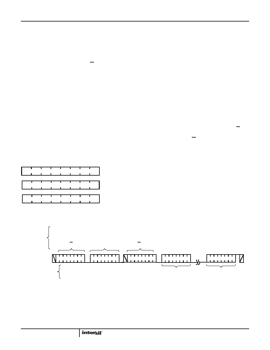
FIGURE 9. SLAVE ADDRESS, WORD ADDRESS, AND DATA
BYTES
SLAVE
ADDRESS BYTE
D7
D6
D5
D2
D4
D3
D1
D0
A0
A7
A2
A4
A3
A1
DATA BYTE
A6
A5
1
10
1
R/W
1
WORD ADDRESS
SIGNALS
FROM THE
MASTER
SIGNALS FROM
THE SLAVE
SIGNAL AT
SDA
S
T
A
R
T
IDENTIFICATION
BYTE WITH
R/W=0
ADDRESS
BYTE
A
C
K
A
C
K
0
S
T
O
P
A
C
K
1
IDENTIFICATION
BYTE WITH
R/W = 1
A
C
K
S
T
A
R
T
LAST READ
DATA BYTE
FIRST READ
DATA BYTE
A
C
K
10
1
1111
10
1
11 11
FIGURE 10. READ SEQUENCE (CSR SLAVE ADDRESS SHOWN)
ISL12032
相关PDF资料 |
PDF描述 |
|---|---|
| VE-J1N-MZ | CONVERTER MOD DC/DC 18.5V 25W |
| VI-J1N-MZ | CONVERTER MOD DC/DC 18.5V 25W |
| VE-J1P-MZ | CONVERTER MOD DC/DC 13.8V 25W |
| ISL1209IU10Z-TK | IC RTC LP SRAM EEPROM 10-MSOP |
| VI-J3Z-EY-F4 | CONVERTER MOD DC/DC 2V 20W |
相关代理商/技术参数 |
参数描述 |
|---|---|
| ISL12057 | 制造商:INTERSIL 制造商全称:Intersil Corporation 功能描述:Low Cost and Low Power I2C RTC Real Time Clock/Calendar |
| ISL12057IBZ | 功能描述:实时时钟 REAL TIME CLK W/ ALARM DS1337 COMP RoHS:否 制造商:Microchip Technology 功能:Clock, Calendar. Alarm RTC 总线接口:I2C 日期格式:DW:DM:M:Y 时间格式:HH:MM:SS RTC 存储容量:64 B 电源电压-最大:5.5 V 电源电压-最小:1.8 V 最大工作温度:+ 85 C 最小工作温度: 安装风格:Through Hole 封装 / 箱体:PDIP-8 封装:Tube |
| ISL12057IBZ-T | 功能描述:实时时钟 REAL TIME CLK W/ ALARM DS1337 COMP RoHS:否 制造商:Microchip Technology 功能:Clock, Calendar. Alarm RTC 总线接口:I2C 日期格式:DW:DM:M:Y 时间格式:HH:MM:SS RTC 存储容量:64 B 电源电压-最大:5.5 V 电源电压-最小:1.8 V 最大工作温度:+ 85 C 最小工作温度: 安装风格:Through Hole 封装 / 箱体:PDIP-8 封装:Tube |
| ISL12057IRUZ-T | 功能描述:实时时钟 REAL TIME CLK W/ ALARM DS1337 COMP RoHS:否 制造商:Microchip Technology 功能:Clock, Calendar. Alarm RTC 总线接口:I2C 日期格式:DW:DM:M:Y 时间格式:HH:MM:SS RTC 存储容量:64 B 电源电压-最大:5.5 V 电源电压-最小:1.8 V 最大工作温度:+ 85 C 最小工作温度: 安装风格:Through Hole 封装 / 箱体:PDIP-8 封装:Tube |
| ISL12057IUZ | 功能描述:实时时钟 REAL TIME CLK W/ ALARM DS1337 COMP RoHS:否 制造商:Microchip Technology 功能:Clock, Calendar. Alarm RTC 总线接口:I2C 日期格式:DW:DM:M:Y 时间格式:HH:MM:SS RTC 存储容量:64 B 电源电压-最大:5.5 V 电源电压-最小:1.8 V 最大工作温度:+ 85 C 最小工作温度: 安装风格:Through Hole 封装 / 箱体:PDIP-8 封装:Tube |
发布紧急采购,3分钟左右您将得到回复。