参数资料
| 型号: | ISL22419WFU8Z-TK |
| 厂商: | Intersil |
| 文件页数: | 2/13页 |
| 文件大小: | 0K |
| 描述: | IC POT DGTL 128TP LN LP 8-MSOP |
| 标准包装: | 1,000 |
| 系列: | XDCP™ |
| 接片: | 128 |
| 电阻(欧姆): | 10k |
| 电路数: | 1 |
| 温度系数: | 标准值 ±50 ppm/°C |
| 存储器类型: | 非易失 |
| 接口: | 4 线 SPI(芯片选择) |
| 电源电压: | 2.7 V ~ 5.5 V |
| 工作温度: | -40°C ~ 125°C |
| 安装类型: | 表面贴装 |
| 封装/外壳: | 8-TSSOP,8-MSOP(0.118",3.00mm 宽) |
| 供应商设备封装: | 8-MSOP |
| 包装: | 带卷 (TR) |
10
FN6311.1
September 8, 2009
The non-volatile IVR and volatile WR registers are
accessible with the same address.
The Access Control Register (ACR) contains information
and control bits described below in Table 2.
The VOL bit (ACR[7]) determines whether the access is to
wiper registers WR or initial value registers IVR.
If VOL bit is 0, the non-volatile IVR register is accessible. If
VOL bit is 1, only the volatile WR is accessible. Note, value
is written to IVR register also is written to the WR. The
default value of this bit is 0.
The SHDN bit (ACR[6]) disables or enables Shutdown mode.
This bit is logically AND with SHDN pin. When this bit is 0, DCP
is in Shutdown mode. Default value of SHDN bit is 1.
The WIP bit (ACR[5]) is read only bit. It indicates that non-
volatile write operation is in progress. The WIP bit can be
read repeatedly after a non-volatile write to determine if the
write has been completed. It is impossible to write to the WR
or ACR while WIP bit is 1.
Shutdown Mode
The device can be put in Shutdown mode either by pulling the
SHDN pin to GND or setting the SHDN bit in the ACR register
to 0. The truth table for Shutdown mode is in Table 3.
SPI Serial Interface
The ISL22419 supports an SPI serial protocol, mode 0. The
device is accessed via the SDI input and SDO output with
data clocked in on the rising edge of SCK, and clocked out
on the falling edge of SCK. CS must be LOW during
communication with the ISL22419. SCK and CS lines are
controlled by the host or master. The ISL22419 operates
only as a slave device.
All communication over the SPI interface is conducted by
sending the MSB of each byte of data first.
Protocol Conventions
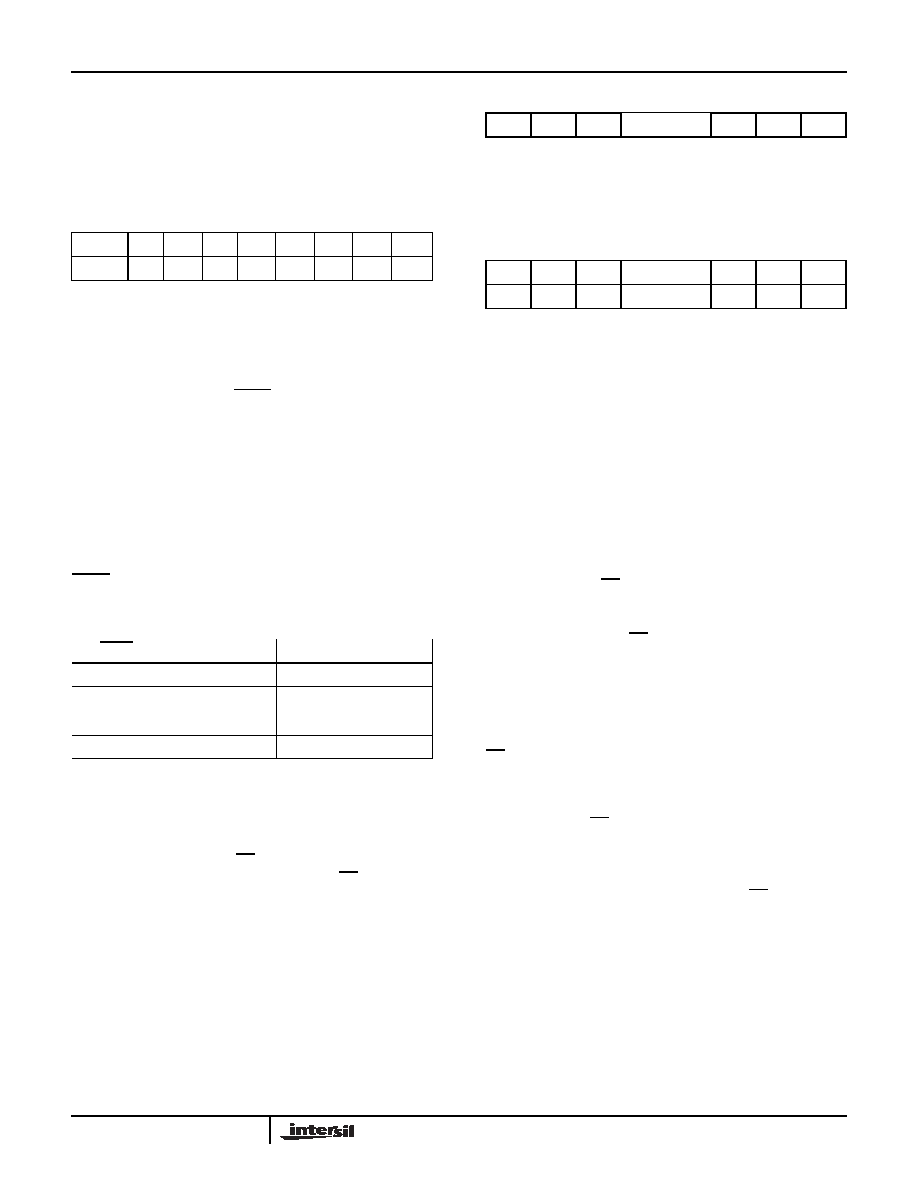
The first byte sent to the ISL22419 from the SPI host is the
Identification Byte. A valid Identification Byte contains 0101
as the four MSBs, with the following four bits set to 0.
TABLE 4. IDENTIFICATION BYTE FORMAT
The next byte sent to the ISL22419 contains the instruction
and register pointer information. The four MSBs are the
instruction and two LSBs are register address (see Table 5).
TABLE 5. IDENTIFICATION BYTE FORMAT
There are only two valid instruction sets:
1011(binary) - is a Read operation
1100(binary) - is a Write operation
There are only two registers address possible for this DCP. If
the R1, R0 bits are zero, then the read or write is to either
the IVR or the WR register (depends of VOL bit at ACR). If
the R1 bit is 1and R0 bit is 0, then the operation is on the
ACR.
Write Operation
A Write operation to the ISL22419 is a three-byte operation.
It requires first, the CS transition from HIGH to LOW, then a
valid Identification Byte, then a valid instruction byte followed
by Data Byte is sent to SDI pin. The host terminates the write
operation by pulling the CS pin from LOW to HIGH. For a
write to address 0 (WR), the byte at address 2 (ACR[7])
determines if the Data Byte is to be written to volatile or both
volatile and non-volatile registers. Refer to “Memory
Description” on page 9 and Figure 12.
The internal non-volatile write cycle starts after rising edge of
CS and takes up to 20ms.
Read Operation
A read operation to the ISL22419 is a three byte operation. It
requires first, the CS transition from HIGH to LOW, then a
valid Identification Byte, then a valid instruction byte followed
by “dummy” Data Byte is sent to SDI pin. The SPI host reads
the data from SDO pin on falling edge of SCK. The host
terminates the read operation by pulling the CS pin from
LOW to HIGH (see Figure 13).
In order to read back the non-volatile IVR, it is recommended
that the application reads the ACR first to verify the WIP bit
is 0. If the WIP bit (ACR[5]) is not 0, the host should repeat
its reading sequence again.
TABLE 2. ACCESS CONTROL REGISTER (ACR)
BIT #
76
5
432
1
0
BIT NAME
VOL
SHDN
WIP
000
0
TABLE 3.
SHDN pin
SHDN bit
Mode
High
1
Normal operation
Low
1
Shutdown
High
0
Shutdown
Low
0
Shutdown
01010000
(MSB)
(LSB)
76543210
I3
I2
I1
I0
0
R1
R0
ISL22419
相关PDF资料 |
PDF描述 |
|---|---|
| VI-27T-MW-S | CONVERTER MOD DC/DC 6.5V 100W |
| ISL22319WFU8Z-TK | IC POT DGTL 128TP LN LP 8-MSOP |
| VI-26X-MW-S | CONVERTER MOD DC/DC 5.2V 100W |
| ICS728MLFT | IC VCXO 27MHZ 3.3V 8-SOIC |
| VI-2TV-MW-S | CONVERTER MOD DC/DC 5.8V 100W |
相关代理商/技术参数 |
参数描述 |
|---|---|
| ISL22424 | 制造商:INTERSIL 制造商全称:Intersil Corporation 功能描述:Dual Digitally Controlled Potentiometer (XDCP?) |
| ISL22424TFR16Z | 功能描述:数字电位计 IC 256 TAP FL RNG IND L SPI DCP 4X4 RoHS:否 制造商:Maxim Integrated 电阻:200 Ohms 温度系数:35 PPM / C 容差:25 % POT 数量:Dual 每 POT 分接头:256 弧刷存储器:Volatile 缓冲刷: 数字接口:Serial (3-Wire, SPI) 描述/功能:Dual Volatile Low Voltage Linear Taper Digital Potentiometer 工作电源电压:1.7 V to 5.5 V 电源电流:27 uA 最大工作温度:+ 125 C 安装风格:SMD/SMT 封装 / 箱体:TQFN-16 封装:Reel |
| ISL22424TFR16Z-TK | 功能描述:数字电位计 IC 256 TAP FL RNG IND DL SPI DCP 4X4 RoHS:否 制造商:Maxim Integrated 电阻:200 Ohms 温度系数:35 PPM / C 容差:25 % POT 数量:Dual 每 POT 分接头:256 弧刷存储器:Volatile 缓冲刷: 数字接口:Serial (3-Wire, SPI) 描述/功能:Dual Volatile Low Voltage Linear Taper Digital Potentiometer 工作电源电压:1.7 V to 5.5 V 电源电流:27 uA 最大工作温度:+ 125 C 安装风格:SMD/SMT 封装 / 箱体:TQFN-16 封装:Reel |
| ISL22424TFV14Z | 功能描述:数字电位计 IC 256 TAP FL RNG IND DL SPI DCP 14LD RoHS:否 制造商:Maxim Integrated 电阻:200 Ohms 温度系数:35 PPM / C 容差:25 % POT 数量:Dual 每 POT 分接头:256 弧刷存储器:Volatile 缓冲刷: 数字接口:Serial (3-Wire, SPI) 描述/功能:Dual Volatile Low Voltage Linear Taper Digital Potentiometer 工作电源电压:1.7 V to 5.5 V 电源电流:27 uA 最大工作温度:+ 125 C 安装风格:SMD/SMT 封装 / 箱体:TQFN-16 封装:Reel |
| ISL22424TFV14Z-TK | 功能描述:数字电位计 IC 256 TAP FL RNG IND DL SPI DCP 14LD RoHS:否 制造商:Maxim Integrated 电阻:200 Ohms 温度系数:35 PPM / C 容差:25 % POT 数量:Dual 每 POT 分接头:256 弧刷存储器:Volatile 缓冲刷: 数字接口:Serial (3-Wire, SPI) 描述/功能:Dual Volatile Low Voltage Linear Taper Digital Potentiometer 工作电源电压:1.7 V to 5.5 V 电源电流:27 uA 最大工作温度:+ 125 C 安装风格:SMD/SMT 封装 / 箱体:TQFN-16 封装:Reel |
发布紧急采购,3分钟左右您将得到回复。