参数资料
| 型号: | ISL23415WFRUZ-T7A |
| 厂商: | Intersil |
| 文件页数: | 6/20页 |
| 文件大小: | 0K |
| 描述: | IC DGTL POT 256POS 10K 10TQFN |
| 产品培训模块: | Solutions for Industrial Control Applications |
| 标准包装: | 1 |
| 系列: | XDCP™ |
| 接片: | 256 |
| 电阻(欧姆): | 10k |
| 电路数: | 1 |
| 温度系数: | 标准值 175 ppm/°C |
| 存储器类型: | 易失 |
| 接口: | 4 线 SPI(芯片选择) |
| 电源电压: | 1.2 V ~ 5.5 V,1.7 V ~ 5.5 V |
| 工作温度: | -40°C ~ 125°C |
| 安装类型: | 表面贴装 |
| 封装/外壳: | 10-UFQFN |
| 供应商设备封装: | 10-UTQFN(2.1x1.6) |
| 包装: | 标准包装 |
| 其它名称: | ISL23415WFRUZ-T7ADKR |
ISL23415
14
FN7780.1
August 16, 2011
DCP Description
Each DCP is implemented with a combination of resistor
elements and CMOS switches. The physical ends of DCP are
equivalent to the fixed terminals of a mechanical potentiometer
(RH and RL pins). The RW pin of the DCP is connected to
intermediate nodes, and is equivalent to the wiper terminal of a
mechanical potentiometer. The position of the wiper terminal
within the DCP is controlled by the 8-bit volatile Wiper Register
(WR). When the WR of a DCP contains all zeroes (WR[7:0] = 00h),
its wiper terminal (RW) is closest to its “Low” terminal (RL). When
the WR register of a DCP contains all ones (WR[7:0] = FFh), its
wiper terminal (RW) is closest to its “High” terminal (RH). As the
value of the WR increases from all zeroes (0) to all ones (255
decimal), the wiper moves monotonically from the position
closest to RL to the position closest to RH. At the same time, the
resistance between RW and RL increases monotonically, while
the resistance between RH and RW decreases monotonically.
While the ISL23415 is being powered up, the WR is reset to 80h
(128 decimal), which locates RW roughly at the center between
RL and RH.
The WR can be read or written to directly using the SPI serial
interface as described in the following sections.
Memory Description
The ISL23415 contains two volatile 8-bit registers: the Wiper
Register (WR) and the Access Control Register (ACR). Memory map
of ISL23415 is in Table 1. The Wiper Register WR at address 0
contains current wiper position of the DCP. The Access Control
Register (ACR) at address 10h contains information and control
bits described in Table 2.
The SDO bit (ACR[1]) configures type of SDO output pin. The
default value of SDO bit is 0 for Push-Pull output. The SDO pin
can be configured as Open Drain output for some applications. In
this case, an external pull-up resistor is required, reference the
Shutdown Function
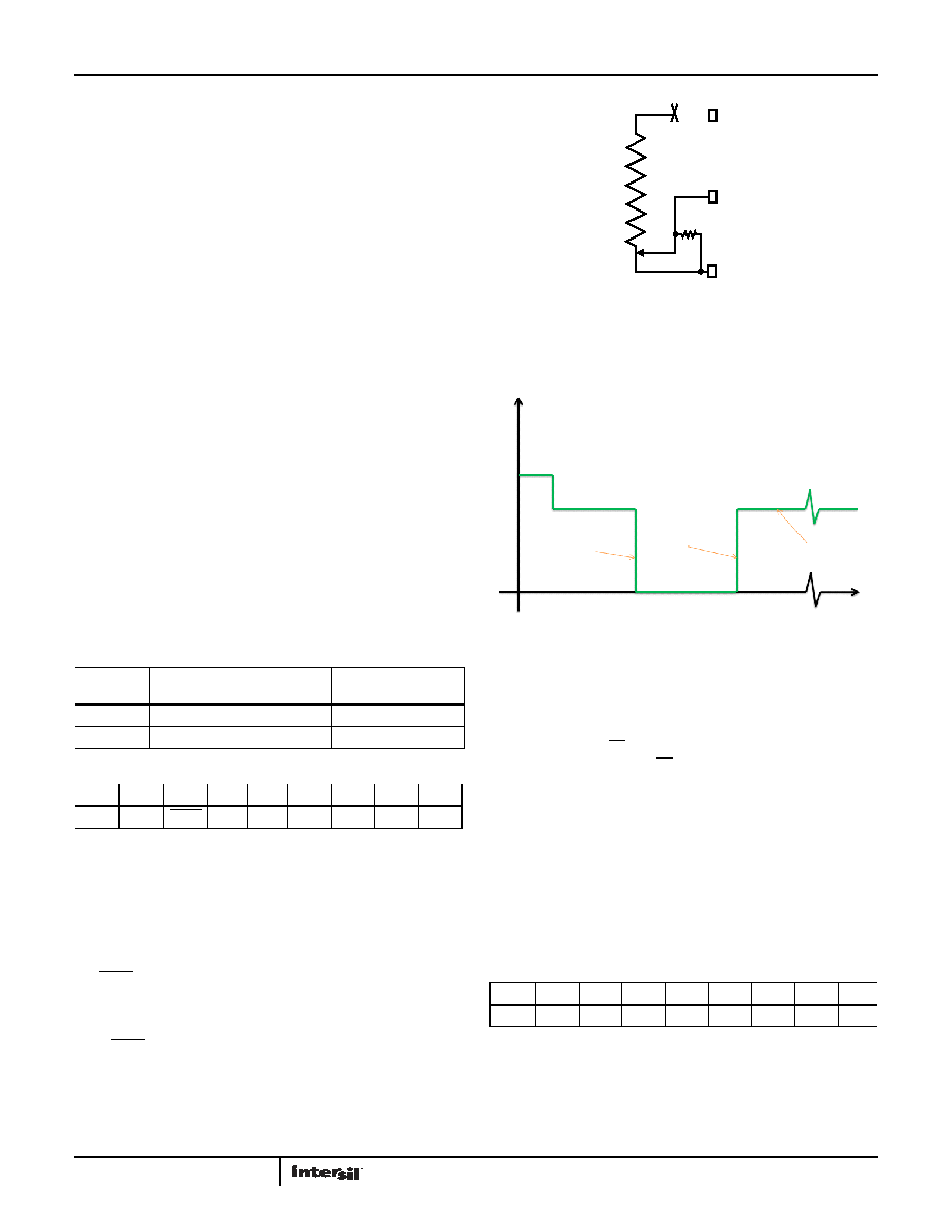
The SHDN bit (ACR[6]) disables or enables shutdown mode for all
DCP channels simultaneously. When this bit is 0, i.e., each DCP is
forced to end-to-end open circuit and each RW shorted to RL
through a 2k serial resistor, as shown in Figure 25. Default value
of the SHDN bit is 1.
When the device enters shutdown, all current DCP WR settings are
maintained. When the device exits shutdown, the wipers will
return to the previous WR settings after a short settling time
(see Figure 26).
SPI Serial Interface
The ISL23415 supports an SPI serial protocol, mode 0. The
device is accessed via the SDI input and SDO output with data
clocked in on the rising edge of SCK, and clocked out on the
falling edge of SCK. CS must be LOW during communication with
the ISL23415. The SCK and CS lines are controlled by the host or
master. The ISL23415 operates only as a slave device.
All communication over the SPI interface is conducted by
sending the MSB of each byte of data first.
Protocol Conventions
The SPI protocol contains Instruction Byte followed by one or more
Data Bytes. A valid Instruction Byte contains instruction as the three
MSBs, with the following five register address bits (see Table 3).
The next byte sent to the ISL23415 is the Data Byte.
Table 4 contains a valid instruction set for ISL23415.
If the [R4:R0] bits are zero or one, then the read or write is to the
WRi register. If the [R4:R0] are 10000, then the operation is to
the ACR.
TABLE 1. MEMORY MAP
ADDRESS
(hex)
VOLATILE
DEFAULT SETTING
(hex)
10
ACR
40
0WR
80
TABLE 2. ACCESS CONTROL REGISTER (ACR)
BIT #
7
6
5
4
3210
NAME
0SHDN
00
0
SDO
0
FIGURE 25. DCP CONNECTION IN SHUTDOWN MODE
FIGURE 26. SHUTDOWN MODE WIPER RESPONSE
TABLE 3. INSTRUCTION BYTE FORMAT
BIT #
7
654321
0
I2
I1
I0
R4
R3
R2
R1
R0
2k
RW
RL
RH
POWER-UP
USER PROGRAMMED
MID SCALE = 80H
SHDN ACTIVATED
SHDN RELEASED
AFTER SHDN
WI
PE
R
VO
LT
AGE,
V
RW
(V)
SHDN MODE
TIME (s)
WIPER RESTORE TO
THE ORIGINAL POSITION
0
相关PDF资料 |
PDF描述 |
|---|---|
| DS1307Z/T&R | IC RTC SERIAL 512K 8-SOIC |
| DS1302S/T&R | IC TIMEKEEPER T-CHARGE 8-SOIC |
| VI-JN4-MZ | CONVERTER MOD DC/DC 48V 25W |
| ISL23315TFRUZ-T7A | IC DGTL POT 256POS 100K 10TQFN |
| DS1390U-3+T&R | IC RTC SPI 3WIRE W/CHRGR 10-MSOP |
相关代理商/技术参数 |
参数描述 |
|---|---|
| ISL23415WFRUZ-TK | 功能描述:数字电位计 IC 256 TAP VOLATILE SPI FL RNG INC DCP 21X16 RoHS:否 制造商:Maxim Integrated 电阻:200 Ohms 温度系数:35 PPM / C 容差:25 % POT 数量:Dual 每 POT 分接头:256 弧刷存储器:Volatile 缓冲刷: 数字接口:Serial (3-Wire, SPI) 描述/功能:Dual Volatile Low Voltage Linear Taper Digital Potentiometer 工作电源电压:1.7 V to 5.5 V 电源电流:27 uA 最大工作温度:+ 125 C 安装风格:SMD/SMT 封装 / 箱体:TQFN-16 封装:Reel |
| ISL23415WFUZ | 功能描述:数字电位计 IC 256 TAP VOLATILE SPI DL FL RNG DCP 10LD RoHS:否 制造商:Maxim Integrated 电阻:200 Ohms 温度系数:35 PPM / C 容差:25 % POT 数量:Dual 每 POT 分接头:256 弧刷存储器:Volatile 缓冲刷: 数字接口:Serial (3-Wire, SPI) 描述/功能:Dual Volatile Low Voltage Linear Taper Digital Potentiometer 工作电源电压:1.7 V to 5.5 V 电源电流:27 uA 最大工作温度:+ 125 C 安装风格:SMD/SMT 封装 / 箱体:TQFN-16 封装:Reel |
| ISL23415WFUZ-T7A | 功能描述:数字电位计 IC 256 TAP VOLATILE SPI DL FL RNG DCP 10LD RoHS:否 制造商:Maxim Integrated 电阻:200 Ohms 温度系数:35 PPM / C 容差:25 % POT 数量:Dual 每 POT 分接头:256 弧刷存储器:Volatile 缓冲刷: 数字接口:Serial (3-Wire, SPI) 描述/功能:Dual Volatile Low Voltage Linear Taper Digital Potentiometer 工作电源电压:1.7 V to 5.5 V 电源电流:27 uA 最大工作温度:+ 125 C 安装风格:SMD/SMT 封装 / 箱体:TQFN-16 封装:Reel |
| ISL23415WFUZ-TK | 功能描述:数字电位计 IC 256 TAP VOLATILE SPI DL FL RNG DCP 10LD RoHS:否 制造商:Maxim Integrated 电阻:200 Ohms 温度系数:35 PPM / C 容差:25 % POT 数量:Dual 每 POT 分接头:256 弧刷存储器:Volatile 缓冲刷: 数字接口:Serial (3-Wire, SPI) 描述/功能:Dual Volatile Low Voltage Linear Taper Digital Potentiometer 工作电源电压:1.7 V to 5.5 V 电源电流:27 uA 最大工作温度:+ 125 C 安装风格:SMD/SMT 封装 / 箱体:TQFN-16 封装:Reel |
| ISL23418 | 制造商:INTERSIL 制造商全称:Intersil Corporation 功能描述:Single, 128-Tap, Low Voltage Digitally Controlled Potentiometer (XDCPa?¢) |
发布紧急采购,3分钟左右您将得到回复。