参数资料
| 型号: | ISL26329FVZ |
| 厂商: | Intersil |
| 文件页数: | 6/23页 |
| 文件大小: | 0K |
| 描述: | IC ADC 12BIT SPI/SRL 16-TSSOP |
| 标准包装: | 960 |
| 位数: | 12 |
| 采样率(每秒): | 250k |
| 数据接口: | 串行,SPI? |
| 转换器数目: | 1 |
| 功率耗散(最大): | 80mW |
| 电压电源: | 单电源 |
| 工作温度: | -40°C ~ 125°C |
| 安装类型: | 表面贴装 |
| 封装/外壳: | 16-TSSOP(0.173",4.40mm 宽) |
| 供应商设备封装: | 16-TSSOP |
| 包装: | 管件 |
| 输入数目和类型: | 8 个单端,单极 |
ISL26320, ISL26321, ISL26322, ISL26323, ISL26324, ISL26325, ISL26329
14
FN8273.1
September 5, 2013
Input Multiplexer
The input of the multiplexer connects the selected analog input
pins to the ADC input. A proprietary sampling circuit significantly
reduces the input drive requirements, resulting in lower overall
cost and board space in addition to improved performance. Note
that the input capacitance is only 2-3pF during the Sampling
phase, changing to 40pF during the Settling phase, resulting in
an average input current of 2.5A and an effective input
capacitance of only 4pF (see Figure 26).
Voltage Reference Input
An external reference voltage must be supplied to theVREF pin to set
the full-scale input range of the converter. The VREF input on these
devices can accept voltages ranging from 2V (nominal) to VDD,
however, they are specified with VREF at a voltage of 5V with VDD at
5V. Note that exceeding VDD by more than 100mV can forward bias
the ESD protection diodes and degrade measurement accuracy due
to leakage current. A lower value voltage reference must be used if
the device is operated with VDD at voltages lower than 5V. If the
VREF pin is tied to the VDD pin, the VREF pin should be decoupled
with a local 1F ceramic capacitor as described in a later paragraph.
for these ADCs. Figure 27 uses the precision ISL21090 voltage
reference, which exhibits exceptionally low drift and low noise.
The ISL21090 must be powered from a supply greater than 4.7V.
Figure 28 illustrates the ISL21010 voltage reference used with
these ADCs. The ISL21010 series voltage references have higher
noise and drift than the ISL21090 devices, but operate at lower
supply voltages. Therefore, these devices can readily be used
when these SAR ADCs operate with VDD at voltages less than 5V.
The outputs of ISL21090 or the ISL21010 devices should be
decoupled with a 1F ceramic capacitor. A 1F, 6.3 V, X7R, 0603
(1608 metric) MLCC type capacitor is recommended for its high
frequency performance. The trace length from the VREF pin to
this capacitor and the voltage reference output should be as
short as possible.
The ISL26320 and ISL26323 devices (packaged in 8 pin SOIC
packages) derive their voltage reference from the VDD pin. To
achieve best performance, the VDD pin of these devices should
be bypassed with the 1F ceramic capacitor mentioned above.
Power-Down/Standby Modes
In order to reduce power consumption between conversions, a
number of user-selectable modes can be utilized by setting the
appropriate bits in the Configuration Register.
Auto Power-down (PD0 = 0) reduces power consumption by
shutting down all portions of the device except the oscillator and
digital interface after completion of a conversion. There is a short
recovery period after CNV is asserted Low (150s with external
reference).
In Auto Sleep mode (PD1 = 1), the device will automatically enter
the low-power Sleep mode at the end of the current conversion.
Recovery from this mode involves only 2.1s and may offer an
alternative to Power-down mode in some applications.
Output Data Format
The converter output word is delivered in two’s complement
format in differential input mode, and straight binary in
single-ended input mode of operation respectively, all MSB-first.
Input exceeding the specified full-scale voltage results in a clipped
output which will not return to in-range values until after the input
signal has returned to the specified allowable voltage range.
Data must be read prior to the completion of the current
conversion to avoid conflict and loss of data, due to overwriting of
the new conversion data into the output register.
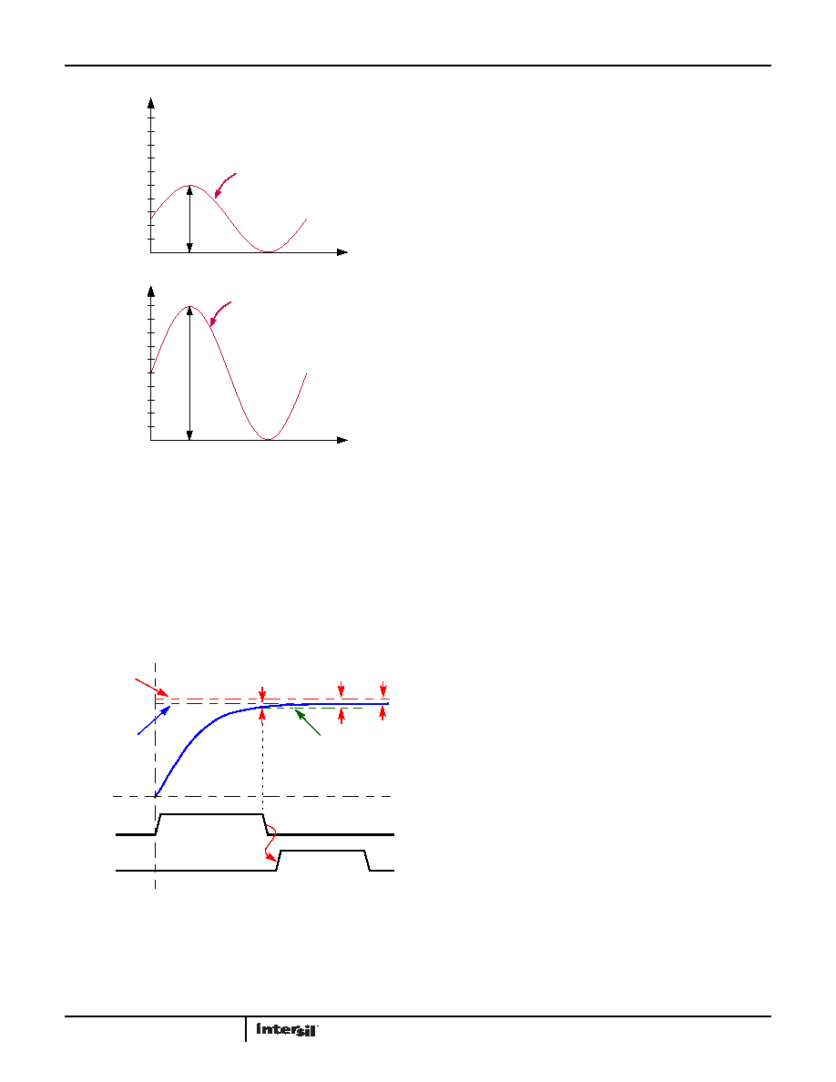
FIGURE 25. RELATIONSHIP BETWEEN VREF AND FULL-SCALE
RANGE FOR SINGLE-ENDED INPUTS
3.0
5.0
2.0
1.0
4.0
AIN
2.5Vp-p
VREF = 2.5V
3.0
5.0
2.0
1.0
4.0
AIN
5Vp-p
VREF = 5V
t
V
t
V
FIGURE 26. INPUT SAMPLING OPERATION
INPUT VOLTAGE
OFFSET ERROR
AC
ERROR
TOTAL
ERROR
DC
ERROR
SETTLING ERROR AND NOISE
SAMPLING PHASE
ETTING PHASE
相关PDF资料 |
PDF描述 |
|---|---|
| ISL2671286IBZ | IC ADC 12BIT SPI/SRL 20K 8SOIC |
| ISL26712IRTZ | IC ADC 12BIT SAR 1MSPS 8-TDFN |
| ISL267450AIUZ | IC INTERFACE |
| ISL267817IUZ | IC INTERFACE |
| ISL32272EIVZ-T | IC TX RS422 QUAD 16TSSOP |
相关代理商/技术参数 |
参数描述 |
|---|---|
| ISL26329FVZ-T | 功能描述:IC ADC 12BIT SPI/SRL 16-TSSOP RoHS:是 类别:集成电路 (IC) >> 数据采集 - 模数转换器 系列:- 产品培训模块:Lead (SnPb) Finish for COTS Obsolescence Mitigation Program 标准包装:250 系列:- 位数:12 采样率(每秒):1.8M 数据接口:并联 转换器数目:1 功率耗散(最大):1.82W 电压电源:模拟和数字 工作温度:-40°C ~ 85°C 安装类型:表面贴装 封装/外壳:48-LQFP 供应商设备封装:48-LQFP(7x7) 包装:管件 输入数目和类型:2 个单端,单极 |
| ISL26329FVZ-T7A | 功能描述:IC ADC 12BIT SPI/SRL 8CH 16TSSOP RoHS:是 类别:集成电路 (IC) >> 数据采集 - 模数转换器 系列:- 产品培训模块:Lead (SnPb) Finish for COTS Obsolescence Mitigation Program 标准包装:1 系列:- 位数:10 采样率(每秒):357k 数据接口:DSP,MICROWIRE?,QSPI?,串行,SPI? 转换器数目:1 功率耗散(最大):830µW 电压电源:单电源 工作温度:-40°C ~ 85°C 安装类型:表面贴装 封装/外壳:10-WFDFN 裸露焊盘 供应商设备封装:10-TDFN-EP(3x3) 包装:剪切带 (CT) 输入数目和类型:2 个单端,单极;2 个单端,双极;1 个差分,单极;1 个差分,双极 产品目录页面:1396 (CN2011-ZH PDF) 其它名称:MAX1395ETB+TCT |
| ISL26708 | 制造商:INTERSIL 制造商全称:Intersil Corporation 功能描述:12-Bit, 10-Bit and 8-Bit, 1MSPS SAR ADCs |
| ISL26708IHZ-T | 功能描述:IC ADC 8BIT SPI/SRL 1M 8-SOT-23 RoHS:是 类别:集成电路 (IC) >> 数据采集 - 模数转换器 系列:- 产品培训模块:Lead (SnPb) Finish for COTS Obsolescence Mitigation Program 标准包装:250 系列:- 位数:12 采样率(每秒):1.8M 数据接口:并联 转换器数目:1 功率耗散(最大):1.82W 电压电源:模拟和数字 工作温度:-40°C ~ 85°C 安装类型:表面贴装 封装/外壳:48-LQFP 供应商设备封装:48-LQFP(7x7) 包装:管件 输入数目和类型:2 个单端,单极 |
| ISL26708IHZ-T7A | 功能描述:IC ADC 8BIT SPI/SRL 1M 8SOT-23 RoHS:是 类别:集成电路 (IC) >> 数据采集 - 模数转换器 系列:- 产品培训模块:Lead (SnPb) Finish for COTS Obsolescence Mitigation Program 标准包装:1 系列:- 位数:10 采样率(每秒):357k 数据接口:DSP,MICROWIRE?,QSPI?,串行,SPI? 转换器数目:1 功率耗散(最大):830µW 电压电源:单电源 工作温度:-40°C ~ 85°C 安装类型:表面贴装 封装/外壳:10-WFDFN 裸露焊盘 供应商设备封装:10-TDFN-EP(3x3) 包装:剪切带 (CT) 输入数目和类型:2 个单端,单极;2 个单端,双极;1 个差分,单极;1 个差分,双极 产品目录页面:1396 (CN2011-ZH PDF) 其它名称:MAX1395ETB+TCT |
发布紧急采购,3分钟左右您将得到回复。