参数资料
| 型号: | ISL26710IRTZ |
| 厂商: | Intersil |
| 文件页数: | 17/21页 |
| 文件大小: | 0K |
| 描述: | IC ADC 10BIT SAR 1MSPS 8-TDFN |
| 标准包装: | 100 |
| 位数: | 10 |
| 采样率(每秒): | 1M |
| 数据接口: | 串行,SPI? |
| 转换器数目: | 1 |
| 功率耗散(最大): | 8.5mW |
| 电压电源: | 单电源 |
| 工作温度: | -40°C ~ 85°C |
| 安装类型: | 表面贴装 |
| 封装/外壳: | 8-WDFN 裸露焊盘 |
| 供应商设备封装: | 8-TDFN(3x3) |
| 包装: | 管件 |
| 输入数目和类型: | 1 个差分,单极 |
ISL26712, ISL26710, ISL26708
5
FN7999.3
September 5, 2012
Absolute Maximum Ratings
Thermal Information
Any Pin to GND . . . . . . . . . . . . . . . . . . . . . . . . . . . . . . . . . . . . . -0.3V to +6.0V
Analog Input to GND. . . . . . . . . . . . . . . . . . . . . . . . . . . . . -0.3V to VDD + 0.3V
Digital I/O to GND. . . . . . . . . . . . . . . . . . . . . . . . . . . . . . . -0.3V to VDD + 0.3V
Digital Input Voltage to GND . . . . . . . . . . . . . . . . . . . . . . -0.3V to VDD + 0.3V
Maximum Current In to Any Pin . . . . . . . . . . . . . . . . . . . . . . . . . . . . . . 10mA
ESD Rating
Human Body Model (Tested per JESD22-A114F) . . . . . . . . . . . . . . . . 8kV
Machine Model (Tested per JESD22-A115B) . . . . . . . . . . . . . . . . . 400V
Charged Device Model (Tested per JESD22-C101E)
TDFN Package . . . . . . . . . . . . . . . . . . . . . . . . . . . . . . . . . . . . . . . . 2.0kV
SOT-23 Package . . . . . . . . . . . . . . . . . . . . . . . . . . . . . . . . . . . . . . . 1.5kV
Latch Up (Tested per JESD78C; Class 2, Level A) . . . . . . . . . . . . . . . 100mA
Thermal Resistance (Typical)
θJA (°C/W)
θJC (°C/W)
8 Ld TDFN Package (Notes 6, 8) . . . . . . . . .
41
6
135
99
Operating Temperature . . . . . . . . . . . . . . . . . . . . . . . . . . . . . -40°C to +85°C
Storage Temperature . . . . . . . . . . . . . . . . . . . . . . . . . . . . . .-65°C to +150°C
Junction Temperature . . . . . . . . . . . . . . . . . . . . . . . . . . . . . . . . . . . . .+150°C
Pb-Free Reflow Profile . . . . . . . . . . . . . . . . . . . . . . . . . . . . . . . see link below
http://www.intersil.com/pbfree/Pb-FreeReflow.asp
CAUTION: Do not operate at or near the maximum ratings listed for extended periods of time. Exposure to such conditions may adversely impact product
reliability and result in failures not covered by warranty.
NOTES:
6.
θJA is measured in free air with the component mounted on a high effective thermal conductivity test board with “direct attach” features. See Tech
Brief TB379.
7.
θJA is measured with the component mounted on a high effective thermal conductivity test board in free air. See Tech Brief TB379 for details.
8. For
θJC, the “case temp” location is the center of the exposed metal pad on the package underside.
9. For
θJC, the “case temp” location is taken at the package top center.
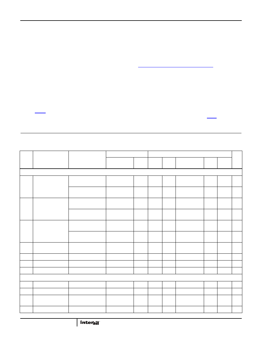
Electrical Specifications VDD = +3.0V to +3.6V, FSCLK = 18MHz, FS = 1MSPS, VREF = 2.0V; VDD = +4.75V to +5.25V, FSCLK = 18MHz,
FS =1MSPS, VREF = 2.5V; VCM = VREF, unless otherwise noted. Typical values are at TA = +25°C. Boldface limits apply over the operating temperature
range, -40°C to +85°C.
SYMBOL
PARAMETER
TEST CONDITIONS
ISL26712
ISL26710
ISL26708
UNITS
MIN
(Note 10)
TYP
MAX
(Note 10)
MIN
(Note 10)
TYP
MAX
(Note 10)
MIN
(Note 10)
TYP
MAX
(Note 10)
DYNAMIC PERFORMANCE
SINAD Signal-to (Noise +
Distortion) Ratio
FIN = 100kHz
VDD = +4.75V to +5.25V
70.0
71.4
61.0
61.6
49.0
49.8
dB
FIN = 100kHz
VDD = +3.0V to +3.6V
68.5
70.5
60.7
61.5
49.0
49.8
dB
THD
Total Harmonic
Distortion
FIN = 100kHz
VDD = +4.75V to +5.25V
-84
-76
-82
-74
-75
-60
dB
FIN = 100kHz
VDD = +3.0V to +3.6V
-84
-74
-82
-72
-73
-60
dB
SFDR Spurious Free Dynamic
Range
FIN = 100kHz
VDD = +4.75V to +5.25V
-87
-76
-82
-76
-68
-60
dB
FIN = 100kHz
VDD = +3.0V to +3.6V
-85
-74
-82
-74
-68
-60
dB
IMD
Intermodulation
Distortion
2nd and 3rd order,
FIN = 90kHz, 110kHz
-89
-83
-81
dB
tpd
Aperture Delay
1
ns
Δtpd Aperture Jitter
15
ps
β3dB Full Power Bandwidth
@ –3dB
15
MHz
DC ACCURACY
NResolution
12
10
8
Bits
INL
Integral Nonlinearity
-1
±0.4
1-0.5
±0.1
0.5
-0.2
±0.03
0.2
LSB
DNL
Differential Nonlinearity Guaranteed no missing
codes
-0.95
±0.3
0.95
-0.5
±0.1
0.5
-0.2
±0.03
0.2
LSB
OFFSET Zero-Code Error
Zero Volt Differential Input
-6
±0.2
6-2.5
±0.2
2.5
-1.25
±0.03
1.25
LSB
相关PDF资料 |
PDF描述 |
|---|---|
| ISL26710IRTZ-T | IC ADC 10BIT SAR 1MSPS 8-TDFN |
| XRT73LC03AIV | IC LIU E3/DS3/STS-1 3CH 120LQFP |
| MS3101A22-20S | CONN RCPT 9POS FREE HNG W/SCKT |
| IDT72V263L10PFI8 | IC FIFO 8192X18 10NS 80QFP |
| VI-B6B-IV-F1 | CONVERTER MOD DC/DC 95V 150W |
相关代理商/技术参数 |
参数描述 |
|---|---|
| ISL26710IRTZ-T | 功能描述:IC ADC 10BIT SAR 1MSPS 8-TDFN RoHS:是 类别:集成电路 (IC) >> 数据采集 - 模数转换器 系列:- 产品培训模块:Lead (SnPb) Finish for COTS Obsolescence Mitigation Program 标准包装:250 系列:- 位数:12 采样率(每秒):1.8M 数据接口:并联 转换器数目:1 功率耗散(最大):1.82W 电压电源:模拟和数字 工作温度:-40°C ~ 85°C 安装类型:表面贴装 封装/外壳:48-LQFP 供应商设备封装:48-LQFP(7x7) 包装:管件 输入数目和类型:2 个单端,单极 |
| ISL26710IRTZ-T7A | 功能描述:模数转换器 - ADC 10 BIT 1MSPS SAR ADC IN 8LD 3x3 RoHS:否 制造商:Texas Instruments 通道数量:2 结构:Sigma-Delta 转换速率:125 SPs to 8 KSPs 分辨率:24 bit 输入类型:Differential 信噪比:107 dB 接口类型:SPI 工作电源电压:1.7 V to 3.6 V, 2.7 V to 5.25 V 最大工作温度:+ 85 C 安装风格:SMD/SMT 封装 / 箱体:VQFN-32 |
| ISL26712 | 制造商:INTERSIL 制造商全称:Intersil Corporation 功能描述:12-Bit, 10-Bit and 8-Bit, 1MSPS SAR ADCs |
| ISL2671286 | 制造商:INTERSIL 制造商全称:Intersil Corporation 功能描述:12-Bit, 20kSPS SAR ADC |
| ISL2671286IBZ | 功能描述:模数转换器 - ADC 12 BIT SINGLE ENDED 20KHZ SAR ADC RoHS:否 制造商:Texas Instruments 通道数量:2 结构:Sigma-Delta 转换速率:125 SPs to 8 KSPs 分辨率:24 bit 输入类型:Differential 信噪比:107 dB 接口类型:SPI 工作电源电压:1.7 V to 3.6 V, 2.7 V to 5.25 V 最大工作温度:+ 85 C 安装风格:SMD/SMT 封装 / 箱体:VQFN-32 |
发布紧急采购,3分钟左右您将得到回复。