参数资料
| 型号: | ISL3333IRZ-T7A |
| 厂商: | Intersil |
| 文件页数: | 26/26页 |
| 文件大小: | 0K |
| 描述: | IC TXRX RS232/485 DL 2PRT 40QFN |
| 产品培训模块: | Solutions for Industrial Control Applications |
| 标准包装: | 250 |
| 类型: | 收发器 |
| 驱动器/接收器数: | 2/2 |
| 规程: | RS232,RS422,RS485 |
| 电源电压: | 3.15 V ~ 3.45 V |
| 安装类型: | 表面贴装 |
| 封装/外壳: | 20-SSOP(0.209",5.30mm 宽) |
| 供应商设备封装: | 20-SSOP |
| 包装: | 带卷 (TR) |
9
FN6362.0
May 27, 2008
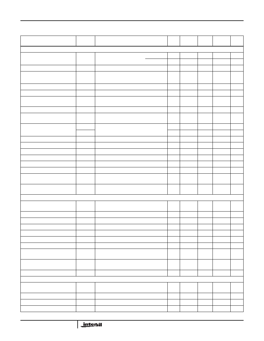
RS-232 DRIVER AND RECEIVER SWITCHING CHARACTERISTICS (SEL = GND, ALL VERSIONS AND SPEEDS)
Driver Output Transition Region
Slew Rate
SR
RL =3kΩ, Measured From
3V to -3V or -3V to 3V
CL ≥ 15pF
Full
-
20
30
V/s
CL ≤ 2500pF
Full
4
9
-
V/s
Driver Output Transition Time
tr, tf
RL =3kΩ, CL = 2500pF, 10% - 90%
Full
0.22
1.2
3.1
s
Driver Propagation Delay
tDPHL
Full
-
1
2
s
tDPLH
Full
-
1.2
2
s
Driver Propagation Delay Skew
tDSKEW
Full
-
300
450
ns
Driver Enable Time (QFN Only)
tDEN
CL = 1000pF
25
-
1500
-
ns
Driver Disable Time (QFN Only)
tDDIS
RL =5kΩ, Measured at VOUT = ±3V,
CL =30pF
25
-
500
-
ns
Driver Enable Time from Shutdown
tDENSD
VOUT = ±3.0V, CL = 1000pF
25
-
25
-
s
Driver Maximum Data Rate
DRD
RL =3kΩ, CL = 500pF, One Transmitter
Switching on Each Port
Full
250
400
-
kbps
Receiver Propagation Delay
tRPHL
Full
-
40
120
ns
tRPLH
Full
-
58
120
ns
Receiver Propagation Delay Skew
tRSKEW
Full
-
18
40
ns
Receiver Maximum Data Rate
DRR
CL = 15pF
Full
0.46
2
-
Mbps
Receiver Enable to Output Low
tZL
QFN Only, CL = 15pF, SW = VCC
Full
-
18
-
ns
Receiver Enable to Output High
tZH
QFN Only, CL = 15pF, SW = GND
Full
-
18
-
ns
Receiver Disable from Output Low
tLZ
QFN Only, CL = 15pF, SW = VCC
Full
-
22
-
ns
Receiver Disable from Output High
tHZ
QFN Only, CL = 15pF, SW = GND
Full
-
22
-
ns
Receiver Enable from Shutdown to
Output Low
tZLSHDN
CL = 15pF, SW = VCC
25
-
60
-
ns
Receiver Enable from Shutdown to
Output High
tZHSHDN CL = 15pF, SW = GND
25
-
20
-
ns
RS-485 DRIVER SWITCHING CHARACTERISTICS (FAST DATA RATE (20Mbps), SEL = VCC, ALL VERSIONS (SPA = VCC if QFN))
Driver Differential Input to Output
Delay
Full
10
20
35
ns
Driver Output Skew
tSKEW
Full
-
2
10
ns
Driver Differential Rise or Fall Time
tR, tF
Full
3
20
30
ns
Driver Enable to Output Low
tZL
Full
-
28
60
ns
Driver Enable to Output High
tZH
Full
-
35
60
ns
Driver Disable from Output Low
tLZ
Full
-
30
60
ns
Driver Disable from Output High
tHZ
Full
-
30
60
ns
Driver Enable from Shutdown to
Output Low
Full
-
100
250
ns
Driver Enable from Shutdown to
Output High
Full
-
290
375
ns
Driver Maximum Data Rate
fMAX
Full
20
35
-
Mbps
RS-485 DRIVER SWITCHING CHARACTERISTICS (MEDIUM DATA RATE (460kbps, QFN ONLY), SEL = VCC, SPA = SPB= GND)
Driver Differential Input to Output
Delay
Full
200
500
1000
ns
Driver Output Skew
tSKEW
Full
-
10
150
ns
Driver Differential Rise or Fall Time
tR, tF
Full
300
660
1100
ns
Driver Enable to Output Low
tZL
Full
-
42
100
ns
Electrical Specifications
Test Conditions: VCC = 3.15V to 3.45V, C1 - C4 = 0.1F, VL = VCC (for QFN only); Unless Otherwise Specified.
Typicals are at VCC = 3.3V, TA =+25°C (Note 7) (Continued)
PARAMETER
SYMBOL
TEST CONDITIONS
TEMP
(°C)
MIN
(Note 11)
TYP
MAX
(Note 11) UNITS
ISL3332, ISL3333
相关PDF资料 |
PDF描述 |
|---|---|
| ISL34321INZ | IC SER/DESER LVDS SERDES 48TQFP |
| ISL34340INZ | IC LNG-RCH VID SERDES 64-EPTQFP |
| ISL34341INZ | IC VIDEO SERDES LONG 64-EPTQFP |
| ISL35111DRZ-TS | IC DE-EMP DRIVER SGL 16QFN |
| ISL35411DRZ-T7 | IC DVR QUAD 46QFN |
相关代理商/技术参数 |
参数描述 |
|---|---|
| ISL34321 | 制造商:INTERSIL 制造商全称:Intersil Corporation 功能描述:16-Bit Long-Reach Video SERDES with Bi-directional Side-Channel |
| ISL34321INZ | 功能描述:串行器/解串器 - Serdes ISL34321INZ16:1 LVDS SERDES W/BCK CH EPAD RoHS:否 制造商:Texas Instruments 类型:Deserializer 数据速率:1.485 Gbit/s 输入类型:ECL/LVDS 输出类型:LVCMOS 输入端数量:1 输出端数量:20 工作电源电压:2.375 V to 2.625 V 工作温度范围:0 C to + 70 C 封装 / 箱体:TQFP-64 |
| ISL34321INZ-T13 | 功能描述:串行器/解串器 - Serdes ISL34321INZ16:1 LVDS SERDES W/BCK CH EPAD RoHS:否 制造商:Texas Instruments 类型:Deserializer 数据速率:1.485 Gbit/s 输入类型:ECL/LVDS 输出类型:LVCMOS 输入端数量:1 输出端数量:20 工作电源电压:2.375 V to 2.625 V 工作温度范围:0 C to + 70 C 封装 / 箱体:TQFP-64 |
| ISL34340 | 制造商:Intersil Corporation 功能描述: |
| ISL34340_0806 | 制造商:INTERSIL 制造商全称:Intersil Corporation 功能描述:WSVGA 24-Bit Long-Reach Video SERDES with Bidirectional Side-Channel |
发布紧急采购,3分钟左右您将得到回复。