参数资料
| 型号: | ISL4089IBZ |
| 厂商: | Intersil |
| 文件页数: | 6/9页 |
| 文件大小: | 0K |
| 描述: | IC VIDEO AMP RESTORED 250MHZ SO8 |
| 标准包装: | 97 |
| 应用: | 通用 |
| 电路数: | 1 |
| -3db带宽: | 300MHz |
| 转换速率: | 300 V/µs |
| 电流 - 电源: | 20mA |
| 电流 - 输出 / 通道: | 100mA |
| 安装类型: | 表面贴装 |
| 封装/外壳: | 8-SOIC(0.154",3.90mm 宽) |
| 供应商设备封装: | 8-SOIC |
| 包装: | 管件 |
| 产品目录页面: | 1234 (CN2011-ZH PDF) |
6
FN6192.1
June 28, 2006
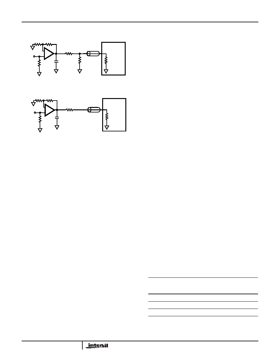
Figure 12A illustrates the AC test circuit used to operate the
video amplifier into a 150
load while providing a 50
matched impedance. Figure 12B illustrates the test circuit for
impedance matching to 75
test equipment.
Application Information
General
The ISL4089 implements the video DC-restore function
using a high performance gain adjustable video amplifier
and a nulling, sample-hold amplifier to establish a user
defined DC reference voltage at the video amplifier output. A
detailed description of the DC-restore function implemented
in the ISL4089 can be found in application note AN1089,
EL4089 and EL4390 DC-Restored Video Amplifier. The
ISL4089 performs the same function with the exception that
it is designed for single supply operation.
Video Amplifier Operation (Figure 13)
The ISL4089 video amplifier (A1) is voltage-feed, high
performance video amplifier designed for +5V operation.
The output stage is capable of swinging to within 10mV of
the negative rail. The differential input stage contains an
internal voltage reference that positions the non-inverting
input DC level (V1) to ~1.2V higher than the negative supply
rail. This offset ensures that the amplifier input DC level is
maintained within the common mode input voltage range.
The amplifier non-inverting gain is given in Equation 1.
DC-Restore Amplifier (Figure 13)
The DC-restore circuit contains a voltage reference amplifier
and an analog switch function that closes the DC-restore
loop under control of the HOLD logic input. The reference
amplifier uses an internal 10mV offset voltage (V2) to enable
the VREF input to sense down to the negative supply. The A2
amplifier output stage operates in a current-feed mode with a
source/sink capability of ±300A (Typ).
A logic “0” at the HOLD input closes switch S1 which closes
the DC-restore loop. The video input AC coupling capacitor,
CX1, acts as a DC hold capacitor (through the 75
termination resistor RX1) to average the current-source
output of amplifier A2. When the DC-restore loop has
reached equilibrium, the DC voltage stored on CX1 will the
value required to force the output voltages at A1 (VOUT) and
A2 (VIN+) according to the following:
and; the DC voltage at the non-inverting input of the video
amplifier A1 is given in Equation 3:
Therefore, if VREF is set to 0V (GND); VOUT = 10mV, and
the DC voltage stored on CX1 is ~1.2V.
The CX1 capacitor value is chosen from the system
requirements. A typical DC-restore application using the
horizontal sync to drive the HOLD pin will result in a 62s
hold time. The typical input bias current to the video amplifier
is 1.2A, so for a 62s hold time, and a 0.01F capacitor, the
output voltage drift is 7.5mV in one line. The restore amplifier
can provide a typical current of 300A to charge capacitor
CX1, so with a 1.2s sampling time, the output can be
corrected by 36mV in each line.
Using a smaller value of CX1 increases both the voltage that
can be corrected, as well as the droop while being held.
Likewise, using a larger value of CX1, reduces the correction
and droop voltages. A sample of charging and droop rates
are shown on the following table.
AC Test Circuits
FIGURE 12A. VIDEO AMPLIFIER AC TEST CIRCUIT FOR 50
FIGURE 12B. BACKTERMINATED TEST CIRCUIT FOR VIDEO
CABLE APPLICATION.
RS
CL
VIN
TEST
86.6
50
118
RG
RF
EQUIPMENT
50
+
-
1. HOLD INPUT = 1
RS
CL
VIN
TEST
75
75
RG
RF
EQUIPMENT
75
+
-
1. HOLD INPUT = 1
V
OUT
V
IN+
1.2V
–
()
1
R
F
R
G
--------
+
=
(EQ. 1)
TABLE OF CHARGE STORAGE CAPACITOR VS DROOP
CHARGING RATES (NOTE)
CAP VALUE
(if)
DROOP IN
62s
(mV)
CHARGE IN
1.2s
(mV)
CHARGE IN
4s
(mV)
10
7.5
36
120
33
2.3
11
36
100
0.75
3.6
12
NOTE: Basic formulae are: V (droop) = Ib+ * (Line time - Sample
time)/Capacitor and V (charge) = IOUT * Sample time/Capacitor
V
OUT(DC)
V
REF
10mV
+
=
(EQ. 2)
V
IN+
V
OUT(DC)
1.2V
+
=
(EQ. 3)
ISL4089
相关PDF资料 |
PDF描述 |
|---|---|
| HFA1145IBZ | IC OPAMP CFA 330MHZ LP 8-SOIC |
| ISL59448IAZ | IC AMP TRIPLE MUX 500MHZ 24-QSOP |
| EL4543ILZ | IC DRIVER TWISTED 350MHZ 20QFN |
| AD669AR | IC DAC 16BIT MONO W/VREF 28-SOIC |
| ISL59440IAZ | IC AMP MULTIPLEX 400MHZ 16-QSOP |
相关代理商/技术参数 |
参数描述 |
|---|---|
| ISL4089IBZ-EVAL | 制造商:Intersil Corporation 功能描述:ISL4089IBZ-EVAL EVALUATION BOARD - Bulk |
| ISL4089IBZ-EVALZ | 功能描述:EVAL BOARD FOR ISL4089IBZ RoHS:是 类别:编程器,开发系统 >> 评估演示板和套件 系列:* 标准包装:1 系列:PCI Express® (PCIe) 主要目的:接口,收发器,PCI Express 嵌入式:- 已用 IC / 零件:DS80PCI800 主要属性:- 次要属性:- 已供物品:板 |
| ISL4089IBZ-T7 | 功能描述:IC VIDEO AMP RESTORED 250MHZ SO8 RoHS:是 类别:集成电路 (IC) >> 线性 - 放大器 - 视频放大器和频缓冲器 系列:- 产品培训模块:Lead (SnPb) Finish for COTS Obsolescence Mitigation Program 标准包装:50 系列:- 应用:TFT-LCD 面板:VCOM 驱动器 输出类型:满摆幅 电路数:1 -3db带宽:35MHz 转换速率:40 V/µs 电流 - 电源:3.7mA 电流 - 输出 / 通道:1.3A 电压 - 电源,单路/双路(±):9 V ~ 20 V,±4.5 V ~ 10 V 安装类型:表面贴装 封装/外壳:8-TSSOP,8-MSOP(0.118",3.00mm 宽)裸露焊盘 供应商设备封装:8-uMax-EP 包装:管件 |
| ISL4089IBZ-T7A | 功能描述:IC VIDEO AMP DC-RESTORED 8SOIC RoHS:是 类别:集成电路 (IC) >> 线性 - 放大器 - 视频放大器和频缓冲器 系列:- 标准包装:1,000 系列:- 应用:驱动器 输出类型:差分 电路数:3 -3db带宽:350MHz 转换速率:1000 V/µs 电流 - 电源:14.5mA 电流 - 输出 / 通道:60mA 电压 - 电源,单路/双路(±):5 V ~ 12 V,±2.5 V ~ 6 V 安装类型:表面贴装 封装/外壳:20-VFQFN 裸露焊盘 供应商设备封装:20-QFN 裸露焊盘(4x4) 包装:带卷 (TR) |
| ISL41334 | 制造商:INTERSIL 制造商全称:Intersil Corporation 功能描述:【15kV ESD Protected, 5V, Two Port, Dual Protocol (RS-232/RS-485) Transceivers |
发布紧急采购,3分钟左右您将得到回复。