- 您现在的位置:买卖IC网 > PDF目录16352 > ISL54063EVAL1Z (Intersil)EVALUATION BOARD FOR ISL54063 PDF资料下载
参数资料
| 型号: | ISL54063EVAL1Z |
| 厂商: | Intersil |
| 文件页数: | 2/15页 |
| 文件大小: | 0K |
| 描述: | EVALUATION BOARD FOR ISL54063 |
| 标准包装: | 1 |
| 主要目的: | 接口,模拟开关 |
| 嵌入式: | 否 |
| 已用 IC / 零件: | ISL54063 |
| 主要属性: | 2 x SPST 模拟开关 |
| 次要属性: | 1.8 V ~ 6.5 V 电源 |
| 已供物品: | 板 |
10
FN6582.1
November 3, 2009
This method is not acceptable for the signal path inputs.
Adding a series resistor to the switch input defeats the
purpose of using a low rON switch. Alternatively, connecting
external Schottky diodes from the V+ rail to the signal pins
will shunt the fault current through the Schottky diode
instead of through the internal ESD diodes, thereby
protecting the switch. These Schottky diodes must be sized
to handle the expected fault current..
Power-Supply Considerations
The ISL54063 and ISL54064 construction is typical of most
single supply CMOS analog switches which have two supply
pins: V+ and GND. V+ and GND provide the CMOS switch
bias and sets their analog voltage limits. Unlike switches with
a 5.5V maximum supply voltage, the ISL54063 and
ISL54064 have a 6.5V maximum supply voltage providing
plenty of head room for the 10% tolerance of 5V supplies
due to overshoot and noise spikes.
The minimum recommended supply voltage is 1.8V. It is
important to note that the input signal range, switching times,
and ON-resistance degrade at lower supply voltages. Refer
to the “Electrical Specifications” tables, beginning on page 4,
and “Typical Performance Curves”, beginning on page 11,
for details.
V+ and GND also power the internal logic and level shifters.
The level shifters convert the input logic levels to V+ and
GND signals levels to drive the analog switch gate terminals.
A high frequency decoupling capacitor placed as close to the
V+ and GND pin as possible is recommended for proper
operation of the switch. A value of 0.1F is highly
recommended.
Negative Signal Swing Capability
The ISL54063 and ISL54064 contains circuitry that allows
the analog switch signal to swing below ground. The device
has an analog signal range of 6.5V below V+ up to the V+
For example, if V+ = 5V, then the analog input signal range is
from -1.5V to +5V. If V+ = 2.7V then the range is from -3.8V
to +2.7V.
Logic-Level Thresholds
This switch family is 1.8V CMOS compatible (0.45V VOLMAX
and 1.35V VOHMIN) over a supply range of 1.8V to 3.3V
is still below the 1.8V CMOS guaranteed low output
maximum level of 0.45V, but noise margin is reduced. At
3.3V the VIH level is 1.4V minimum. While this is above the
1.8V CMOS guaranteed high output minimum of 1.35V
under most operating conditions the switch will recognize
this as a valid logic high.
The digital input stages draw supply current whenever the
digital input voltage is not at one of the supply rails. Driving
the digital input signals from GND to V+ with a fast transition
time minimizes power dissipation. The ISL54063 and
ISL54064 have been designed to minimize the supply
current whenever the digital input voltage is not driven to the
supply rails (0V to V+). For example driving the device with
2.85V logic high while operating with a 4.2V supply the
device draws only 1A of current.
High-Frequency Performance
In 50
Ω systems, the ISL54063 and ISL54064 have an ON
switch -3dB bandwidth of 60MHz (see Figure 19). The
frequency response is very consistent over a wide V+ range,
and for varying analog signal levels.
An OFF switch acts like a capacitor across the open
terminals and AC couples higher frequencies, resulting in
signal feed-through from a switch’s input to its output.
Off-Isolation is the resistance to this feed-through. Crosstalk
indicates the amount of feed-through from one switch
channel to another switch channel. Figure 20 details the high
Off-Isolation and Crosstalk rejection provided by this part. At
100kHz, Off-Isolation is about 60dB in 50
Ω systems,
decreasing approximately 20dB per decade as frequency
increases. At 1MHz, Crosstalk is about -75dB in 50
Ω
systems, decreasing approximately 20dB per decade as
frequency increases.
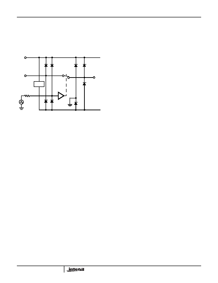
Leakage Considerations
Reverse ESD protection diodes are internally connected
between each analog-signal pin, V+ and GND. One of these
diodes conducts if any analog signal exceeds the
recommended analog signal range.
Virtually all the analog switch leakage current comes from
the ESD diodes and reversed biased junctions in the switch
cell. Although the ESD diodes on a given signal pin are
identical and therefore fairly well balanced, they are reverse
biased differently. Each is biased to either the +Ring or -Ring
and the analog input signal. This means their leakages will
vary as the signal varies. The difference in the two diode
leakages to the +Ring or -Ring and the reverse biased
junctions at the internal switch cell constitutes the
analog-signal-path leakage current.
GND
VCOMx
VNCx
V+
LOGIC
INPUTS
VNOx
-RING
+RING
CLAMP
1k
Ω
OR
FIGURE 8. OVERVOLTAGE PROTECTION
ISL54063, ISL54064
相关PDF资料 |
PDF描述 |
|---|---|
| UPA1E332MHD1TN | CAP ALUM 3300UF 25V 20% RADIAL |
| ADM6713RAKSZ-REEL7 | IC SUPERVISOR MPU 2.63V SC70-4 |
| AFK687M35H32T-F | CAP ALUM 680UF 35V 20% SMD |
| 6435092-2 | MT-RJ TO SC SIMPLEX LLEAD |
| ADM6713TAKSZ-REEL7 | IC SUPERVISOR OD 3.08V SC70-4 |
相关代理商/技术参数 |
参数描述 |
|---|---|
| ISL54063IRTZ | 功能描述:IC SWITCH SPDT DUAL 10TDFN RoHS:是 类别:集成电路 (IC) >> 接口 - 模拟开关,多路复用器,多路分解器 系列:- 产品培训模块:Lead (SnPb) Finish for COTS Obsolescence Mitigation Program 标准包装:36 系列:- 功能:多路复用器 电路:2 x 4:1 导通状态电阻:75 欧姆 电压电源:单/双电源 电压 - 电源,单路/双路(±):2 V ~ 12 V,±2 V ~ 6 V 电流 - 电源:- 工作温度:0°C ~ 70°C 安装类型:表面贴装 封装/外壳:20-SOIC(0.295",7.50mm 宽) 供应商设备封装:20-SOIC W 包装:管件 |
| ISL54063IRTZ-T | 功能描述:IC SWITCH SPDT DUAL 10TDFN RoHS:是 类别:集成电路 (IC) >> 接口 - 模拟开关,多路复用器,多路分解器 系列:- 产品培训模块:Lead (SnPb) Finish for COTS Obsolescence Mitigation Program 标准包装:36 系列:- 功能:多路复用器 电路:2 x 4:1 导通状态电阻:75 欧姆 电压电源:单/双电源 电压 - 电源,单路/双路(±):2 V ~ 12 V,±2 V ~ 6 V 电流 - 电源:- 工作温度:0°C ~ 70°C 安装类型:表面贴装 封装/外壳:20-SOIC(0.295",7.50mm 宽) 供应商设备封装:20-SOIC W 包装:管件 |
| ISL54063IRUZ-T | 功能描述:IC SWITCH SPDT DUAL 10TQFN RoHS:是 类别:集成电路 (IC) >> 接口 - 模拟开关,多路复用器,多路分解器 系列:- 产品培训模块:Lead (SnPb) Finish for COTS Obsolescence Mitigation Program 标准包装:36 系列:- 功能:多路复用器 电路:2 x 4:1 导通状态电阻:75 欧姆 电压电源:单/双电源 电压 - 电源,单路/双路(±):2 V ~ 12 V,±2 V ~ 6 V 电流 - 电源:- 工作温度:0°C ~ 70°C 安装类型:表面贴装 封装/外壳:20-SOIC(0.295",7.50mm 宽) 供应商设备封装:20-SOIC W 包装:管件 |
| ISL54064 | 制造商:INTERSIL 制造商全称:Intersil Corporation 功能描述:1.8V to +6.5V, Sub-ohm, Dual SPST |
| ISL54064EVAL1Z | 功能描述:EVALUATION BOARD FOR ISL54064 RoHS:是 类别:编程器,开发系统 >> 评估演示板和套件 系列:- 标准包装:1 系列:PCI Express® (PCIe) 主要目的:接口,收发器,PCI Express 嵌入式:- 已用 IC / 零件:DS80PCI800 主要属性:- 次要属性:- 已供物品:板 |
发布紧急采购,3分钟左右您将得到回复。