- 您现在的位置:买卖IC网 > PDF目录11791 > ISL54102CQZ (Intersil)IC TMDS REGEN W/MUX 128MQFP PDF资料下载
参数资料
| 型号: | ISL54102CQZ |
| 厂商: | Intersil |
| 文件页数: | 9/21页 |
| 文件大小: | 0K |
| 描述: | IC TMDS REGEN W/MUX 128MQFP |
| 标准包装: | 66 |
| 应用: | 显示器 |
| 接口: | I²C |
| 电源电压: | 3 V ~ 3.6 V |
| 封装/外壳: | 128-BFQFP |
| 供应商设备封装: | 128-MQFP(14x20) |
| 包装: | 托盘 |
| 安装类型: | 表面贴装 |
| 产品目录页面: | 1244 (CN2011-ZH PDF) |
17
FN6275.5
June 4, 2008
planes and 100
Ω with respect to each other. Failure to
meet this requirement will increase reflections, shrinking
the available eye.
Avoid vias for all 3 high speed TMDS pairs. Vias add
inductance which causes a discontinuity in the
characteristic impedance of the trace. Keep all the traces
on the top (or the bottom) of the PCB. The TMDS clock
can have vias if necessary, since it is lower speed and less
critical. If you must use a via, ensure the vias are
symmetrical (put identical vias in both lines of the
differential pair).
For each TMDS channel, the trace lengths of the 3 TMDS
pairs (0, 1 and 2) should ideally be the same to reduce
inter channel skew introduced by the board.
The trace length of the clock pair is not critical at all.
Since the clock is only used as a frequency reference, its
phase/delay is inconsequential. In addition, since the
TMDS clock frequency is 1/10th the pixel rate, the clock
signal itself is much more noise-immune. So liberties
(such as vias and circuitous paths) can be taken when
routing the clock lines.
Minimize capacitance on all TMDS lines. The lower the
capacitance, the sharper the rise and fall times.
Maintain a constant, solid ground (or power) plane under
the 3 high speed TMDS signals. Do not route the signals
over gaps in the ground plane or over other traces.
Ideally each supply should be bypassed to ground with a
0.1F capacitor. Minimize trace length and vias to
minimize inductance and maximize noise rejection.
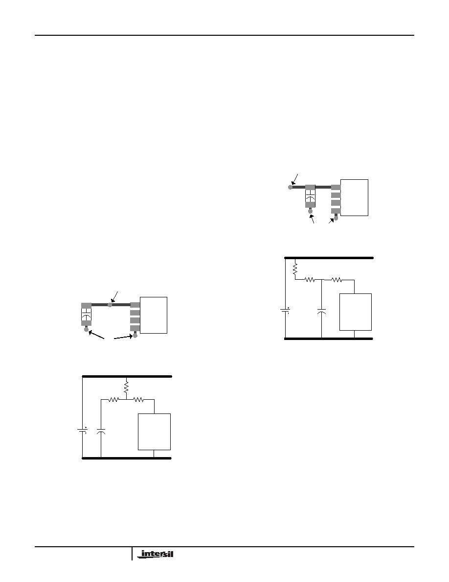
Figure 12 demonstrates a common but non-ideal PCB
layout and its equivalent circuit. The additional trace
resistance between the bypass capacitor and the power
supply/IC reduces its effectiveness. Figure 13
demonstrates a better layout. In this case there is still
series trace resistance (it is impossible to completely
eliminate it), but now it is being put to good use, as part of
a “T” filter, attenuating supply noise before it gets to the IC,
and reducing the amount of IC-generated noise that gets
injected into the supply. Follow the good supply bypassing
rules shown in Figure 13 to the extent possible.
CBYPASS
RTRACE
V
+
RTRACE
IC
V
+
GND
GROUND PLANE
POWER PLANE
CBYPASS
IC
V
+
GND
VIAS
TO
GND
VIA TO
POWER
PLANE
EQUIVALENT CIRCUIT
RVIA
FIGURE 12. SUB-OPTIMAL BYPASS CAPACITOR LAYOUT
FIGURE 13. OPTIMAL (“T”) BYPASS CAPACITOR LAYOUT
CBYPASS
RTRACE
V
+
RTRACE
IC
V
+
GND
GROUND PLANE
CBYPASS
IC
V
+
GND
VIAS
TO
GND
VIA TO
POWER
PLANE
EQUIVALENT CIRCUIT
POWER PLANE
RVIA
ISL54100, ISL54101, ISL54102
相关PDF资料 |
PDF描述 |
|---|---|
| IA186ES-PTQ100I-R-03 | IC MCU 8/16BIT 40MHZ 100TQFP |
| PI7C8152BMAE | IC PCI-PCI BRIDGE 2PORT 160-MQFP |
| DS80C310-MCG+ | IC MCU HI SPEED 25MHZ 40-DIP |
| MS27468E21B41S | CONN RCPT 41POS JAM NUT W/SCKT |
| AT32UC3C2512C-A2UR | IC MCU AVR32 512K FLASH 64TQFP |
相关代理商/技术参数 |
参数描述 |
|---|---|
| ISL54103 | 制造商:INTERSIL 制造商全称:Intersil Corporation 功能描述:DDC Accelerator (DDCA) |
| ISL54103IHZ-T7 | 功能描述:接口 - 专用 ISL55016IRTZFREE DIF GAIN BLOCK(75OHM ZIN RoHS:否 制造商:Texas Instruments 产品类型:1080p60 Image Sensor Receiver 工作电源电压:1.8 V 电源电流:89 mA 最大功率耗散: 最大工作温度:+ 85 C 安装风格:SMD/SMT 封装 / 箱体:BGA-59 |
| ISL54103IHZ-T7A | 功能描述:接口 - 专用 ISL55020IRZ FL DIFFR CFA W/LW DISTORTIO RoHS:否 制造商:Texas Instruments 产品类型:1080p60 Image Sensor Receiver 工作电源电压:1.8 V 电源电流:89 mA 最大功率耗散: 最大工作温度:+ 85 C 安装风格:SMD/SMT 封装 / 箱体:BGA-59 |
| ISL54105A | 制造商:INTERSIL 制造商全称:Intersil Corporation 功能描述:TMDS Regenerator |
| ISL54105ACRZ | 功能描述:IC TMDS REGENERATOR 72-QFN RoHS:是 类别:集成电路 (IC) >> 接口 - 专用 系列:- 标准包装:3,000 系列:- 应用:PDA,便携式音频/视频,智能电话 接口:I²C,2 线串口 电源电压:1.65 V ~ 3.6 V 封装/外壳:24-WQFN 裸露焊盘 供应商设备封装:24-QFN 裸露焊盘(4x4) 包装:带卷 (TR) 安装类型:表面贴装 产品目录页面:1015 (CN2011-ZH PDF) 其它名称:296-25223-2 |
发布紧急采购,3分钟左右您将得到回复。