参数资料
| 型号: | ISL54225IRUZ-T7A |
| 厂商: | Intersil |
| 文件页数: | 2/18页 |
| 文件大小: | 0K |
| 描述: | IC MULTIPLEXER DUAL 2:1 10TQFN |
| 标准包装: | 1 |
| 功能: | 多路复用器 |
| 电路: | 2 x 2:1 |
| 导通状态电阻: | 20 欧姆 |
| 电压电源: | 单电源 |
| 电压 - 电源,单路/双路(±): | 2.7 V ~ 5.25 V |
| 电流 - 电源: | 45µA |
| 工作温度: | -40°C ~ 85°C |
| 安装类型: | 表面贴装 |
| 封装/外壳: | 10-UFQFN |
| 供应商设备封装: | 10-UTQFN(1.8x1.40) |
| 包装: | 标准包装 |
| 其它名称: | ISL54225IRUZ-T7ADKR |
10
FN7627.0
July 2, 2010
The HS1 channel switches are active (turned ON)
whenever the SEL voltage is logic “0”(Low) and the OE
voltage is logic “0”(Low).
The HS2 channel switches are active (turned ON)
whenever the SEL voltage is logic “1” (High) and the OE
voltage is logic “0” (Low).
OVERVOLTAGE PROTECTION (OVP)
The maximum normal operating signal range for the HSx
switches is from 0V to 3.6V. For normal operation, the
signal voltage should not be allowed to exceed these
voltage levels or go below ground by more than -0.3V.
However, in the event that a positive voltage > 3.8V
(typ) to 5.25V, such as the USB 5V VBUS voltage, gets
shorted to one or both of the COM+ and COM- pins or a
negative voltage < -0.5V (typ) to -5V gets shorted to one
or both of the COM pins, the ISL54225 has OVP circuitry
to detect the overvoltage condition and open the SPDT
switches to prevent damage to the USB down-stream
transceivers connected at the signal pins (HS1D-,
HS1D+, HS2D-, HS2D+).
The OVP and power-off protection circuitry allows the
COM pins (D-, D+) to be driven up to 5.25V while the
VDD supply voltage is in the range of 0V to 5.25V. In this
condition, the part draws < 100A of ICOMx and IDD
current and causes no stress to the IC. In addition, the
SPDT switches are OFF and the fault voltage is isolated
from the other side of the switch.
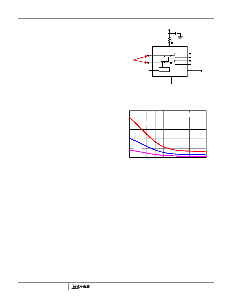
External VDD Series Resistor to Limit IDD Current
during Negative OVP Condition
A 100Ω to 1kΩ resistor in series with the VDD pin (see
Figure 7) is required to limit the IDD current draw from the
system power supply rail during a negative OVP fault event.
With a negative -5V fault voltage at both COM pins, the
graph in Figure 8 shows the IDD current draw for
different external resistor values for supply voltages of
2.7V, 3.6V, and 5.25V. With a 500Ω resistor, the current
draw is limited to around 5mA. When the negative fault
voltage is removed, the IDD current will return to it’s
normal operation current of 25A to 45A.
The series resistor also provides improved ESD and
latch-up immunity. During an overvoltage transient
event (such as occurs during system level IEC 61000
ESD testing), substrate currents can be generated in
the IC that can trigger parasitic SCR structures to turn
ON, creating a low impedance path from the VDD
power supply to ground. This will result in a significant
amount of current flow in the IC, which can potentially
create a latch-up state or permanently damage the IC.
The external VDD resistor limits the current during this
over-stress situation and has been found to prevent
latch-up or destructive damage for many overvoltage
transient events.
Under normal operation, the low microamp IDD current
of the IC produces an insignificant voltage drop across
the series resistor resulting in no impact to switch
operation or performance.
ISL54225 Operation
The following will discuss using the ISL54225 shown in
POWER
The power supply connected at the VDD pin provides the
DC bias voltage required by the ISL54225 part for proper
operation. The ISL54225 can be operated with a VDD
voltage in the range of 2.7V to 5.25V.
For lowest power consumption you should use the lowest
VDD supply.
A 0.01F or 0.1F decoupling capacitor should be
connected from the VDD pin to ground to filter out any
power supply noise from entering the part. The
capacitor should be located as close to the VDD pin as
possible.
In a typical application, VDD will be in the range of
2.8V to 4.3V and will be connected to the battery or
LDO of the portable media device.
FIGURE 7. VDD SERIES RESISTOR TO LIMIT IDD
CURRENT DURING NEGATIVE OVP AND
FOR ENHANCED ESD AND LATCH-UP
IMMUNITY
FIGURE 8. NEGATIVE OVP IDD CURRENT vs
RESISTOR VALUE vs VSUPPLY
SEL
D+
D-
GND
OVP
LOGIC
VDD
OE
HSD1+
100Ω to 1kΩ
VSUPPLY
C
PROTECTION
RESISTOR
HSD1-
IDD
-5V
FAULT
VOLTAGE
HSD2+
HSD2-
0
5
10
15
20
25
100 200 300 400 500 600 700 800 900 1k
RESISTOR (Ω)
I DD
(mA)
VCOM+ = VCOM- = -5V
2.7V
3.6V
5.25V
ISL54225
相关PDF资料 |
PDF描述 |
|---|---|
| ISL54226IRUZ-T | IC USB SWITCH DPST OVP 8TQFN |
| ISL54227IRTZ | IC USB SWITCH DUAL DPST 10TDFN |
| ISL54228IRUZ-T | IC USB SWITCH DPST OVP 8TQFN |
| ISL54230IRTZ | IC SWITCH QUAD DPDT 32TQFN |
| ISL54233IRUZ-T | IC INTERFACE |
相关代理商/技术参数 |
参数描述 |
|---|---|
| ISL54226 | 制造商:INTERSIL 制造商全称:Intersil Corporation 功能描述:High-Speed USB 2.0 (480Mbps) DPST Switch with Overvoltage Protection (OVP) and Dedicated Charger Port Detection |
| ISL54226_10 | 制造商:INTERSIL 制造商全称:Intersil Corporation 功能描述:High-Speed USB 2.0 (480Mbps) DPST Switch with Overvoltage Protection (OVP) and Dedicated Charger Port Detection |
| ISL54226IRTZEVAL1Z | 功能描述:BOARD EVAL FOR ISL5426A MUX RoHS:是 类别:编程器,开发系统 >> 评估演示板和套件 系列:- 标准包装:1 系列:PCI Express® (PCIe) 主要目的:接口,收发器,PCI Express 嵌入式:- 已用 IC / 零件:DS80PCI800 主要属性:- 次要属性:- 已供物品:板 |
| ISL54226IRTZ-T | 功能描述:IC USB SWITCH DPST OVP 8TDFN RoHS:是 类别:集成电路 (IC) >> 接口 - 模拟开关,多路复用器,多路分解器 系列:- 其它有关文件:STG4159 View All Specifications 标准包装:5,000 系列:- 功能:开关 电路:1 x SPDT 导通状态电阻:300 毫欧 电压电源:双电源 电压 - 电源,单路/双路(±):±1.65 V ~ 4.8 V 电流 - 电源:50nA 工作温度:-40°C ~ 85°C 安装类型:表面贴装 封装/外壳:7-WFBGA,FCBGA 供应商设备封装:7-覆晶 包装:带卷 (TR) |
| ISL54226IRTZ-T7A | 功能描述:IC USB SWITCH DPST OVP 8TDFN RoHS:是 类别:集成电路 (IC) >> 接口 - 模拟开关,多路复用器,多路分解器 系列:- 应用说明:Ultrasound Imaging Systems Application Note 产品培训模块:Lead (SnPb) Finish for COTS Obsolescence Mitigation Program 标准包装:250 系列:- 功能:开关 电路:单刀单掷 导通状态电阻:48 欧姆 电压电源:单电源 电压 - 电源,单路/双路(±):2.7 V ~ 5.5 V 电流 - 电源:5µA 工作温度:0°C ~ 70°C 安装类型:表面贴装 封装/外壳:48-LQFP 供应商设备封装:48-LQFP(7x7) 包装:托盘 |
发布紧急采购,3分钟左右您将得到回复。